- 您現(xiàn)在的位置:買賣IC網(wǎng) > PDF目錄371003 > MC10319DW (MOTOROLA INC) Hex Inverter Buffers/Drivers With Open-Collector High-Voltage Outputs 14-CFP -55 to 125 PDF資料下載
參數(shù)資料
| 型號(hào): | MC10319DW |
| 廠商: | MOTOROLA INC |
| 元件分類: | ADC |
| 英文描述: | Hex Inverter Buffers/Drivers With Open-Collector High-Voltage Outputs 14-CFP -55 to 125 |
| 中文描述: | 8-BIT FLASH METHOD ADC, PARALLEL ACCESS, PDSO28 |
| 封裝: | PLASTIC, SO-28 |
| 文件頁數(shù): | 4/20頁 |
| 文件大?。?/td> | 338K |
| 代理商: | MC10319DW |
MC10319
4
MOTOROLA ANALOG IC DEVICE DATA
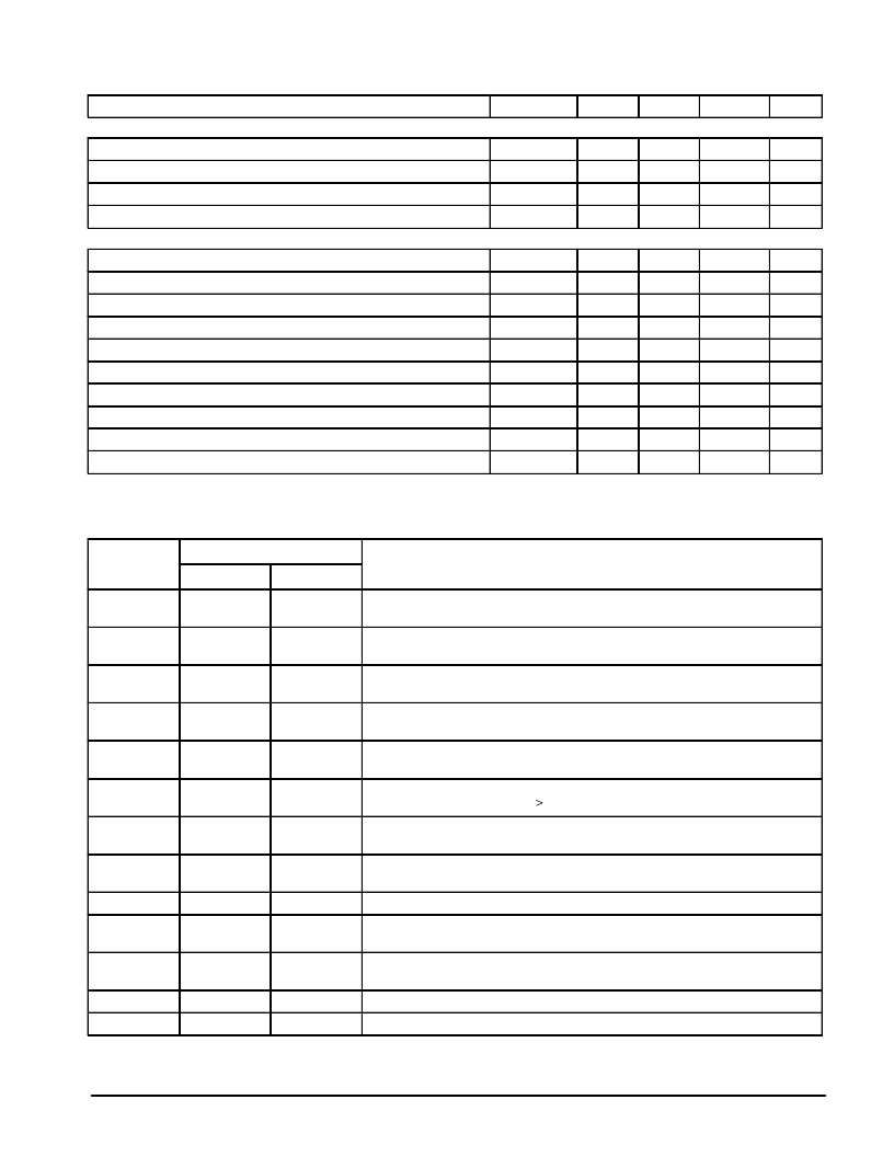
TIMING CHARACTERISTICS
(TA = 25
°
C, VCC = + 5.0 V, VEE = – 5.2 V, VRT = + 1.0 V, VRB = – 1.0 V,
see System Timing Diagram, Figure 1.)
Characteristic
Symbol
Min
Typ
Max
Unit
INPUTS
Min Clock Pulse Width – High
tCKH
tCKL
tR,F
fCLK
–
5.0
–
ns
Min Clock Pulse Width – Low
–
15
–
ns
Max Clock Rise, Fall Time
–
100
–
ns
Clock Frequency
0
30
25
MHz
OUTPUTS
New Data Valid from Clock Low
tCKDV
tAD
tH
tEHZ
tELZ
tEHZ
tELZ
tEDV
tEDV
ttr
–
19
–
ns
Aperture Delay
–
4.0
–
ns
Hold Time
–
6.0
–
ns
Data High to 3–State from Enable Low*
–
27
–
ns
Data Low to 3–State from Enable Low*
–
18
–
ns
Data High to 3–State from Enable High*
–
32
–
ns
Data Low to 3–State from Enable High*
–
18
–
ns
Valid Data from Enable High (Pin 20 = 0 V)*
–
15
–
ns
Valid Data from Enable Low (Pin 19 = 5.0 V)*
–
16
–
ns
Output Transition Time* (10% to 90%)
–
8.0
–
ns
*See Figure 2 for output loading.
PIN FUNCTION DESCRIPTION
Function
Pin
Description
P Suffix
DW Suffix
VRM
1
1
The midpoint of the reference resistor ladder. Bypassing can be done at this point to
improve performance at high frequencies.
GND
2, 12
16, 22
2, 13, 17
18, 25, 26
Digital ground. The pins should be connected directly together, and through a low
impedance path to the power supply.
OVR
3
3
Overrange output. Indicates Vin is more positive than VRT 1/2 LSB. This output does
not have 3–state capability.
D7–D0
4 to 10, 21
4 to 10, 24
Digital Outputs. D7 (Pin 4) is the MSB. D
(Pin 21 or 24) is the LSB. LS–TTL
compatible with 3–state capability.
VCC(D)
11, 17
11, 12
19, 20
Power supply for the digital section. +5.0 V,
±
10% required. Reference to digital
ground.
VEE
13
14
Negative power supply. Nominally – 5.2 V, it can range from – 3.0 to – 6.0 V, and must
be more negative than VRB by
1.3 V. Reference to analog ground.
Vin
14
15
Signal voltage input. This voltage is compared to the reference to generate a digital
equivalent. Input impedance is nominally 16 to 33K in parallel with 36 pF.
VCC(A)
15
16
Power supply for the analog section. +5.0 V,
±
10% required. Reference to analog
ground.
CLK
18
21
Clock input. TTL compatible.
EN
19
22
Enable input. TTL compatible, a logic 1 (and EN at a logic 0) enables the data outputs.
A logic 0 puts the outputs in a 3–state mode.
EN
20
23
Enable input. TTL compatible, a logic 0 (and EN at a logic 1) enables the data outputs.
A logic 1 puts the outputs in a 3–state mode.
VRB
VRT
23
27
The bottom (most negative point) of the internal reference resistor ladder.
24
28
The top (most positive point) of the internal reference resistor ladder.
相關(guān)PDF資料 |
PDF描述 |
|---|---|
| MC10319P | Hex Buffers/Drivers With Open-Collector High-Voltage Outputs 14-CDIP -55 to 125 |
| MC10524 | Hex Inverter Buffers/Drivers With Open-Collector High-Voltage Outputs 20-LCCC -55 to 125 |
| MC10E122FN | CAP 1200UF 350V ELECT TUP SERIES |
| MC10E122 | 9-BIT BUFFER |
| MC100E122FN | 9-BIT BUFFER |
相關(guān)代理商/技術(shù)參數(shù) |
參數(shù)描述 |
|---|---|
| MC1031P | 制造商:Rochester Electronics LLC 功能描述:- Bulk |
| MC1032P | 制造商:Rochester Electronics LLC 功能描述:- Bulk |
| MC1033300 | 制造商:MISCELLANEOUS 功能描述: |
| MC-10333-00 | 制造商:EAO International 功能描述:SWITCH SPNO |
| MC1033P | 制造商:Rochester Electronics LLC 功能描述:- Bulk |
發(fā)布緊急采購,3分鐘左右您將得到回復(fù)。