- 您現(xiàn)在的位置:買賣IC網(wǎng) > PDF目錄371004 > MC10H117P (MOTOROLA INC) Dual 2-Wide 2-3-input OR-AND/OR-AND Gate PDF資料下載
參數(shù)資料
| 型號: | MC10H117P |
| 廠商: | MOTOROLA INC |
| 元件分類: | 通用總線功能 |
| 英文描述: | Dual 2-Wide 2-3-input OR-AND/OR-AND Gate |
| 中文描述: | 10H SERIES, DUAL 5-INPUT OR-AND/OR-AND-INVERT GATE, PDIP16 |
| 封裝: | PLASTIC, DIP-16 |
| 文件頁數(shù): | 1/3頁 |
| 文件大?。?/td> | 96K |
| 代理商: | MC10H117P |

SEMICONDUCTOR TECHNICAL DATA
2–223
REV 5
Motorola, Inc. 1996
3/93
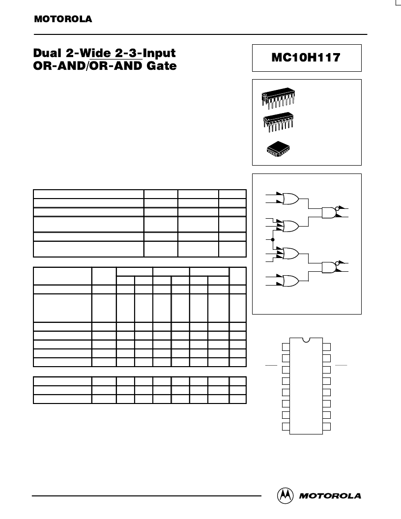
The MC10H117 dual 2–wide 2–3–input OR–AND/OR–AND–Invert gate is a
general purpose logic element designed for use in data control, such as digital
multiplexing or data distribution. Pin 9 is common to both gates. This MECL 10H
part is a functional/pinout duplication of the standard MECL 10K family part,
with 100% improvement in propagation delay, and no increase in power–supply
current.
Propagation Delay, 1.0 ns Typical
Power Dissipation 100 mW/Gate Typical (same as MECL 10K)
Improved Noise Margin 150 mV (Over Operating Voltage and
Temperature Range)
Voltage Compensated
MECL 10K–Compatible
MAXIMUM RATINGS
Characteristic
Symbol
Rating
Unit
Power Supply (VCC = 0)
Input Voltage (VCC = 0)
Output Current— Continuous
VEE
VI
Iout
–8.0 to 0
Vdc
0 to VEE
50
100
Vdc
— Surge
mA
Operating Temperature Range
TA
Tstg
0 to +75
°
C
°
C
°
C
Storage Temperature Range— Plastic
— Ceramic
–55 to +150
–55 to +165
ELECTRICAL CHARACTERISTICS
(VEE = –5.2 V
±
5%) (See Note)
0
°
25
°
75
°
Characteristic
Symbol
Min
Max
Min
Max
Min
Max
Unit
Power Supply Current
IE
IinH
—
29
—
26
—
29
mA
μ
A
Input Current High
Pins 4, 5, 12, 13
Pins 6, 7, 10, 11
Pin 9
—
—
—
465
545
710
—
—
—
275
320
415
—
—
—
275
320
415
Input Current Low
IinL
VOH
VOL
VIH
VIL
0.5
—
0.5
—
0.3
—
μ
A
Vdc
High Output Voltage
–1.02
–0.84
–0.98
–0.81
–0.92
–0.735
Low Output Voltage
–1.95
–1.63
–1.95
–1.63
–1.95
–1.60
Vdc
High Input Voltage
–1.17
–0.84
–1.13
–0.81
–1.07
–0.735
Vdc
Low Input Voltage
–1.95
–1.48
–1.95
–1.48
–1.95
–1.45
Vdc
AC PARAMETERS
Propagation Delay
tpd
tr
tf
0.45
1.35
0.45
1.35
0.5
1.5
ns
Rise Time
0.5
1.5
0.5
1.6
0.5
1.7
ns
Fall Time
0.5
1.5
0.5
1.6
0.5
1.7
ns
NOTE:
Each MECL 10H series circuit has been designed to meet the dc specifications shown in the test table,
after thermal equilibrium has been established. The circuit is in a test socket or mounted on a printed circuit
board and transverse air flow greater than 500 Iinear fpm is maintained. Outputs are terminated through
a 50–ohm resistor to –2.0 volts.
LOGIC DIAGRAM
DIP
PIN ASSIGNMENT
VCC1
AOUT
AOUT
A1IN
A1IN
A2IN
A2IN
VEE
VCC2
BOUT
BOUT
B1IN
B1IN
B2IN
B2IN
A2IN, B2IN
16
15
14
13
12
11
10
9
1
2
3
4
5
6
7
8
12
13
11
10
9
7
6
5
4
3
2
14
15
VCC1 = PIN 1
VCC2 = PIN 16
VEE = PIN 8
L SUFFIX
CERAMIC PACKAGE
CASE 620–10
P SUFFIX
PLASTIC PACKAGE
CASE 648–08
FN SUFFIX
PLCC
CASE 775–02
Pin assignment is for Dual–in–Line Package.
For PLCC pin assignment, see the Pin Conversion
Tables on page 6–11 of the Motorola MECL Data
Book (DL122/D).
相關(guān)PDF資料 |
PDF描述 |
|---|---|
| MC10H123FN | Triple 4-3-3-Input Bus Driver |
| MC10H123 | Triple 4-3-3-Input Bus Driver |
| MC10H123L | Triple 4-3-3-Input Bus Driver |
| MC10H123P | Triple 4-3-3-Input Bus Driver |
| MC10H131P | Dual D Type Master-Slave Flip-Flop |
相關(guān)代理商/技術(shù)參數(shù) |
參數(shù)描述 |
|---|---|
| MC10H117PG | 功能描述:邏輯門 Dual 2-3-Input OR-AND/OR-AND Invert RoHS:否 制造商:Texas Instruments 產(chǎn)品:OR 邏輯系列:LVC 柵極數(shù)量:2 線路數(shù)量(輸入/輸出):2 / 1 高電平輸出電流:- 16 mA 低電平輸出電流:16 mA 傳播延遲時間:3.8 ns 電源電壓-最大:5.5 V 電源電壓-最小:1.65 V 最大工作溫度:+ 125 C 安裝風(fēng)格:SMD/SMT 封裝 / 箱體:DCU-8 封裝:Reel |
| MC10H118P | 制造商:Rochester Electronics LLC 功能描述:- Bulk |
| MC10H119FN | 制造商:ONS 功能描述:ON SEMICONDUCTOR NXC5C 制造商:Motorola Inc 功能描述:Logic Circuit, 3/3/3/4-IN OR-AND, 20 Pin, Plastic, LDCC |
| MC10H119L | 制造商:Motorola Inc 功能描述: 制造商:Motorola Inc 功能描述:Logic Circuit, 3/3/3/4-IN OR-AND, 16 Pin, Ceramic, DIP |
| MC10H121C | 制造商:Motorola Inc 功能描述: |
發(fā)布緊急采購,3分鐘左右您將得到回復(fù)。