- 您現(xiàn)在的位置:買(mǎi)賣(mài)IC網(wǎng) > PDF目錄371008 > MC13110AFB (MOTOROLA INC) UNIVERSAL NARROWBAND FM RECEIVER INTEGRATED CIRCUIT PDF資料下載
參數(shù)資料
| 型號(hào): | MC13110AFB |
| 廠商: | MOTOROLA INC |
| 元件分類(lèi): | 無(wú)繩電話(huà)/電話(huà) |
| 英文描述: | UNIVERSAL NARROWBAND FM RECEIVER INTEGRATED CIRCUIT |
| 中文描述: | TELECOM, CORDLESS, RF AND BASEBAND CIRCUIT, PQFP52 |
| 封裝: | PLASTIC, QFP-52 |
| 文件頁(yè)數(shù): | 33/68頁(yè) |
| 文件大小: | 1316K |
| 代理商: | MC13110AFB |
第1頁(yè)第2頁(yè)第3頁(yè)第4頁(yè)第5頁(yè)第6頁(yè)第7頁(yè)第8頁(yè)第9頁(yè)第10頁(yè)第11頁(yè)第12頁(yè)第13頁(yè)第14頁(yè)第15頁(yè)第16頁(yè)第17頁(yè)第18頁(yè)第19頁(yè)第20頁(yè)第21頁(yè)第22頁(yè)第23頁(yè)第24頁(yè)第25頁(yè)第26頁(yè)第27頁(yè)第28頁(yè)第29頁(yè)第30頁(yè)第31頁(yè)第32頁(yè)當(dāng)前第33頁(yè)第34頁(yè)第35頁(yè)第36頁(yè)第37頁(yè)第38頁(yè)第39頁(yè)第40頁(yè)第41頁(yè)第42頁(yè)第43頁(yè)第44頁(yè)第45頁(yè)第46頁(yè)第47頁(yè)第48頁(yè)第49頁(yè)第50頁(yè)第51頁(yè)第52頁(yè)第53頁(yè)第54頁(yè)第55頁(yè)第56頁(yè)第57頁(yè)第58頁(yè)第59頁(yè)第60頁(yè)第61頁(yè)第62頁(yè)第63頁(yè)第64頁(yè)第65頁(yè)第66頁(yè)第67頁(yè)第68頁(yè)

MC13110A/B MC13111A/B
33
MOTOROLA ANALOG IC DEVICE DATA
Receive Audio Path
The Rx Audio signal path begins at “Rx Audio In” and goes
through the IC to “E Out”. The “Rx Audio In”, “Scr Out”, and
“E In” pins are all ac–coupled. This signal path consists of
filters; programmable Rx gain adjust, Rx mute, and volume
control, and finally the expander. The typical maximum
output voltage at “E Out” should be approximately 0 dBV @
THD = 5.0% .
Figures 71 to 73 represent the receive audio path filter
response. The filter response attenuation is very sharp above
3900 Hz, which is the cutoff frequency. Inband (audio),
out–of–band, and ripple characteristics are also shown in
these graphs.
The group delay (Figure 75) has a peak around 6.5 kHz.
This spike is formed by rapid change in the phase at the
frequency. In practice this does not cause a problem since
the signal is attenuated by at least 50 dB.
The output capability at “Scr Out” and “E Out” are shown in
Figures 76, 77, and 78. The results were obtained by
increasing the input level for 2.0% distortion at the outputs.
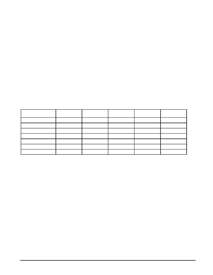
In Figure 70, noise data for the Rx audio path is shown.
At Scr Out, the noise level clearly rises when the scrambler is
enabled. However, assuming a nominal output level of –20
dBV (100 mVrms) at the 0 dB gain setting, the noise floor is
more than 56 dB below the audio signal. However, the noise
data at E Out and SA Out is much more improved.
Speaker Amp
The Speaker Amp is an inverting rail–to–rail operational
amplifier. The noninverting input is connected to the internal
VB reference. External resistors and capacitors are used to
set the gain and frequency response. The “SA In” input pin
must be ac–coupled. The typical output voltage at “SA Out” is
2.6 Vpp with a 130
load. The speaker amp response is
shown in Figures 79 and 80.
Data Amp Comparator
The data amp comparator is an inverting hysteresis
comparator. Its open collector output has an internal 100 k
pull–up resistor. A band pass filter is connected between the
“Det Out” pin and the “DA In” pin with component values as
shown in the Application Circuit schematic. The “DA In” input
signal needs to be ac–coupled, too.
áááááááááááááááááááááááááááááááá
áááááááááááááááááááááááááááááááá
Scrambler
(dB)
(dB)
(dBV)
(dBV)
(dBV)
off/on
muted
muted
< –95
< –95
< –95
off
–9.0
–14
–92
< –95
< –95
off
0
0
–85
< –95
< –95
off
1.0
16
–76
< –95
< –95
on (MC13110A/B)
–9.0
–14
–85
< –95
< –95
on (MC13110A/B)
0
0
–77
< –95
< –95
on (MC13110A/B)
10
16
–66
< –95
< –95
相關(guān)PDF資料 |
PDF描述 |
|---|---|
| MC13110AFTA | UNIVERSAL NARROWBAND FM RECEIVER INTEGRATED CIRCUIT |
| MC13110BFB | UNIVERSAL NARROWBAND FM RECEIVER INTEGRATED CIRCUIT |
| MC13111AFB | UNIVERSAL NARROWBAND FM RECEIVER INTEGRATED CIRCUIT |
| MC13110BFTA | UNIVERSAL NARROWBAND FM RECEIVER INTEGRATED CIRCUIT |
| MC13111AFTA | UNIVERSAL NARROWBAND FM RECEIVER INTEGRATED CIRCUIT |
相關(guān)代理商/技術(shù)參數(shù) |
參數(shù)描述 |
|---|---|
| MC13110AFTA | 制造商:MOTOROLA 制造商全稱(chēng):Motorola, Inc 功能描述:UNIVERSAL NARROWBAND FM RECEIVER INTEGRATED CIRCUIT |
| MC13110BFB | 制造商:MOTOROLA 制造商全稱(chēng):Motorola, Inc 功能描述:UNIVERSAL NARROWBAND FM RECEIVER INTEGRATED CIRCUIT |
| MC13110BFTA | 制造商:Motorola 功能描述:MOTOROLA 9942 |
| MC13111AFB | 制造商:MOTOROLA 制造商全稱(chēng):Motorola, Inc 功能描述:UNIVERSAL NARROWBAND FM RECEIVER INTEGRATED CIRCUIT |
| MC13111AFTA | 制造商:MOTOROLA 制造商全稱(chēng):Motorola, Inc 功能描述:UNIVERSAL CORDLESS TELEPHONE SUBSYSTEM IC |
發(fā)布緊急采購(gòu),3分鐘左右您將得到回復(fù)。