- 您現(xiàn)在的位置:買賣IC網(wǎng) > PDF目錄379305 > MC141800AT (MOTOROLA INC) LCD Segment/Common Driver PDF資料下載
參數(shù)資料
| 型號: | MC141800AT |
| 廠商: | MOTOROLA INC |
| 元件分類: | 顯示驅(qū)動器 |
| 英文描述: | LCD Segment/Common Driver |
| 中文描述: | LIQUID CRYSTAL DISPLAY DRIVER, UUC236 |
| 封裝: | TAB-236 |
| 文件頁數(shù): | 5/32頁 |
| 文件大?。?/td> | 541K |
| 代理商: | MC141800AT |
第1頁第2頁第3頁第4頁當前第5頁第6頁第7頁第8頁第9頁第10頁第11頁第12頁第13頁第14頁第15頁第16頁第17頁第18頁第19頁第20頁第21頁第22頁第23頁第24頁第25頁第26頁第27頁第28頁第29頁第30頁第31頁第32頁
3–281
MC141800A
MOTOROLA
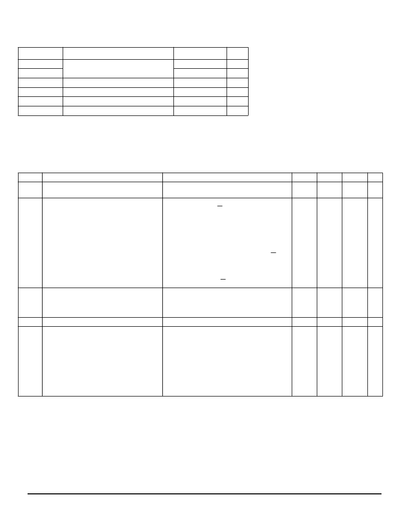
MAXIMUM RATINGS*
(Voltages Referenced to V
SS
, T
A
=25C)
Symbol
Parameter
Value
Unit
AV
DD
,DV
DD
V
CC
V
in
I
Supply Voltage
-0.3 to +4.0
V
V
SS
-0.3 to V
SS
+16.5
V
SS
-0.3 to V
DD
+0.3
25
V
Input Voltage
V
Current Drain Per Pin Excluding V
DD
and V
SS
Operating Temperature
mA
T
A
T
stg
-30 to +85
C
Storage Temperature Range
-65 to +150
C
* Maximum Ratings are those values beyond which damage to the device may occur. Functional
operation should be restricted to the limits in the Electrical Characteristics tables or Pin Descrip-
tion section.
V
SS
= AV
SS
= DV
SS
(DV
SS
= V
SS
of Digital circuit, AV
SS
= V
SS
of Analogue Circuit)
V
DD
= AV
DD
= DV
DD
(DV
DD
= V
DD
of Digital circuit, AV
DD
= V
DD
of Analogue Circuit)
This device contains circuitry to protect the inputs
against damage due to high static voltages or elec-
tric fields; however, it is advised that normal precau-
tions to be taken to avoid application of any voltage
higher than maximum rated voltages to this high
impedance circuit. For proper operation it is recom-
mended that V
in
and V
out
be constrained to the
range V
SS
< or = (V
in
or V
out
) < or = V
DD
. Reliability
of operation is enhanced if unused input are con-
nected to an appropriate logic voltage level (e.g.,
either V
SS
or V
DD
). Unused outputs must be left
open. This device may be light sensitive. Caution
should be taken to avoid exposure of this device to
any light source during normal operation. This
device is not radiation protected.
ELECTRICAL CHARACTERISTICS
(Voltage Referenced to V
SS
, V
DD
=2.4 to 3.5V, T
A
=25C)
Symbol
Parameter
Test Condition
Min
Typ
Max
Unit
DV
DD
AV
DD
I
AC
Logic Circuit Supply Voltage Range
Voltage Generator Circuit Supply Voltage Range
(Absolute value referenced to V
SS
)
2.4
2.4
3.0
-
3.5
3.5
V
V
I
DP
I
SB
I
ICON
Access Mode Supply Current Drain
(AV
DD
+ DV
DD
Pins)
Display Mode Supply Current Drain
(AV
DD
+ DV
DD
Pins)
Standby Mode Supply Current Drain
(AV
DD
+ DV
DD
Pins)
Icon Mode Supply Current Drain
(AV
DD
+ DV
DD
Pins)
LCD Driving Internal DC/DC Converter Output
(V
CC
Pin)
V
DD
=3.0V, Internal DC/DC Converter On, 5X DC/DC
Converter Enabled, R/W accessing, T
cyc
=1MHz,
Osc. Freq.=50KHz, Display On.
V
DD
=3.0V, Internal DC/DC Converter On, 5X Con-
verter Enabled, R/W Halt, Osc. Freq.=50KHz, Dis-
play On.
V
DD
=3.0V, Display off, Oscillator Disabled, R/W halt.
V
DD
=3.0V, Internal Oscillator, Oscillator Enabled,
Display On, Icon On, R/W halt, Freq.=50KHz.
-
-
-
-
500
300
TBD
TBD
TBD
TBD
1
25
μ
A
μ
A
μ
A
μ
A
V
CC
V
LCD
V
ICON
V
OH1
LCD Driving Voltage Input (V
CC
Pin)
Low Power Icon mode Voltage
Display On, DC/DC Converter Enabled, Osc. Freq.=
50KHz, Internal Regulator Enabled, Divider Enabled.
Internal DC/DC Converter Disabled.
7
7
15
15
16.5
16.5
V
V
-
2
-
V
V
OL1
V
R1
V
R2
Output High Voltage
(D0-D7, OSC2)
Output Low Voltage
(D0-D7, OSC2)
LCD Driving Voltage Source (V
R
Pin)
LCD Driving Voltage Source (V
R
Pin)
I
out
=100
μ
A
I
out
=100
μ
A
Internal Regulator Enabled (V
R
voltage depends on
Int/Ext Contrast Control)
Internal Regulator Disable.
0.9*V
DD
0
0
-
-
-
-
Floating
V
DD
0.1*V
DD
V
CC
-0.5
-
V
V
V
V
相關PDF資料 |
PDF描述 |
|---|---|
| MCC141800AZ | LCD Segment/Common Driver |
| MC14194BCL | 4-Bit Bidirectional Universal Shift Register |
| MC14194BCP | MILITARY DIGITAL SIGNAL PROCESSORS 132-BQFP -55 to 125 |
| MC14194BD | 4-Bit Bidirectional Universal Shift Register |
| MC143421FU | PCI Bus Interface |
相關代理商/技術參數(shù) |
參數(shù)描述 |
|---|---|
| MC-141M | 制造商:Panasonic Industrial Company 功能描述:BAG |
| MC142236DW | 制造商:Motorola Inc 功能描述:142236DW |
| MC-1425-15-18 | 制造商:RRE 制造商全稱:RRE 功能描述:Miniature Close Differential Reed Switch |
| MC-142M | 制造商:Panasonic Industrial Company 功能描述:BAG |
| MC1430G | 制造商:Rochester Electronics LLC 功能描述:- Bulk |
發(fā)布緊急采購,3分鐘左右您將得到回復。