- 您現(xiàn)在的位置:買賣IC網(wǎng) > PDF目錄371013 > MC145050P (MOTOROLA INC) 10-Bit A/D Converter with Serial Interface PDF資料下載
參數(shù)資料
| 型號: | MC145050P |
| 廠商: | MOTOROLA INC |
| 元件分類: | ADC |
| 英文描述: | 10-Bit A/D Converter with Serial Interface |
| 中文描述: | 11-CH 10-BIT SUCCESSIVE APPROXIMATION ADC, SERIAL ACCESS, PDIP20 |
| 封裝: | PLASTIC, DIP-20 |
| 文件頁數(shù): | 2/15頁 |
| 文件大小: | 181K |
| 代理商: | MC145050P |

MC145050 MC145051
2
MOTOROLA WIRELESS SEMICONDUCTOR
SOLUTIONS DEVICE DATA
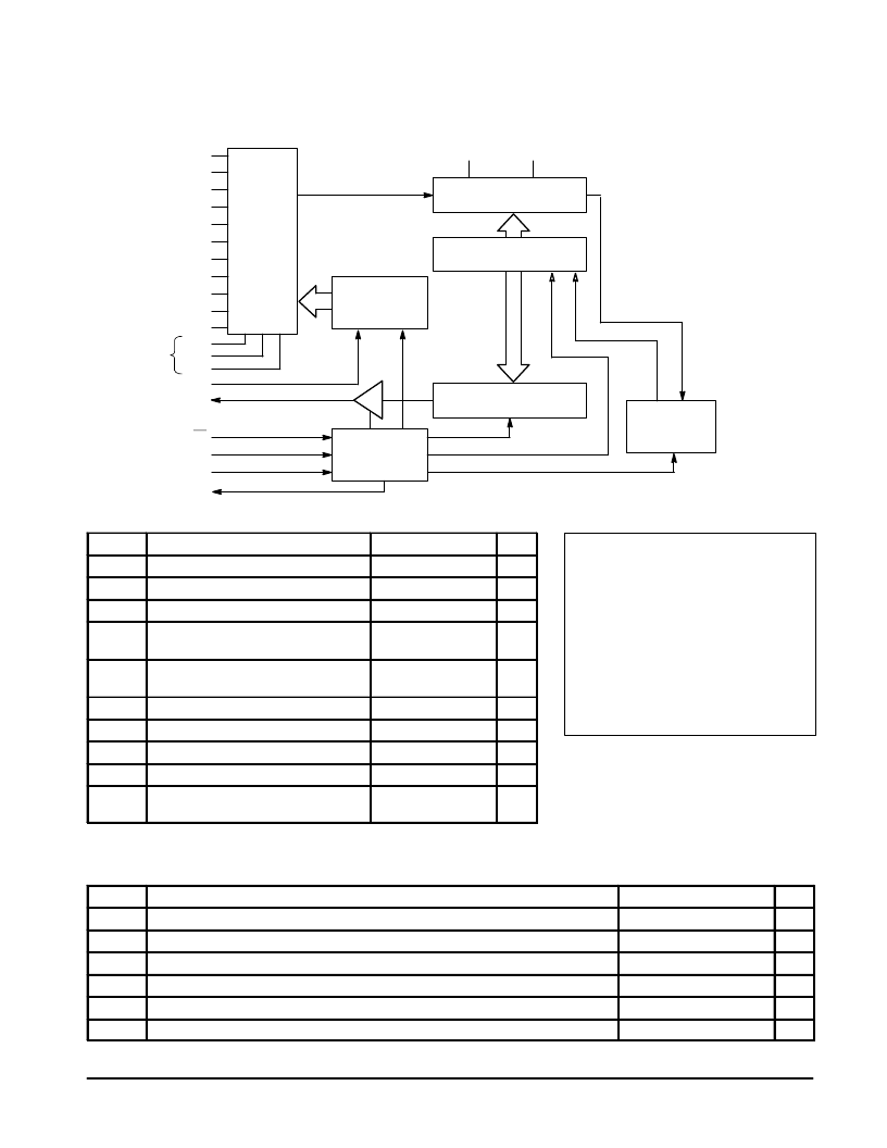
BLOCK DIAGRAM
SUCCESSIVE APPROXIMATION
REGISTER
1
2
3
4
5
6
7
8
9
11
12
17
16
19
15
18
19
10-BIT RC DAC
WITH SAMPLE AND HOLD
DATA REGISTER
14
13
VAG
Vref
AUTO-ZEROED
COMPARATOR
MUX ADDRESS
REGISTER
DIGITAL CONTROL
LOGIC
AN0
AN1
AN2
AN3
AN4
AN5
AN6
AN7
AN8
AN9
AN10
AN11
AN12
AN13
Din
Dout
CS
SCLK
EOC (MC145051 ONLY)
ADCLK (MC145050 ONLY)
MUX OUT
PIN 20 = VDD
PIN 10 = VSS
ANALOG
MUX
INTERNAL
TEST
VOLTAGES
ABSOLUTE MAXIMUM RATINGS
Symbol
Parameter
Value
Unit
VDD
Vref
VAG
Vin
DC Supply Voltage (Referenced to VSS)
DC Reference Voltage
– 0.5 to + 6.0
V
VAG to VDD + 0.1
VSS – 0.1 to Vref
VSS – 0.5 to
VDD + 0.5
V
Analog Ground
V
DC Input Voltage, Any Analog or Digital
Input
V
Vout
DC Output Voltage
VSS – 0.5 to
VDD + 0.5
V
Iin
Iout
DC Input Current, per Pin
±
20
mA
DC Output Current, per Pin
±
25
mA
IDD, ISS
Tstg
TL
DC Supply Current, VDD and VSS Pins
Storage Temperature
±
50
mA
– 65 to 150
°
C
Lead Temperature, 1 mm from Case for
10 Seconds
260
°
C
* Maximum Ratings are those values beyond which damage to the device may occur. Func-
tional operation should be restricted to the Operation Ranges below..
OPERATION RANGES
(Applicable to Guaranteed Limits)
Symbol
Parameter
Value
Unit
VDD
Vref
VAG
VAI
Vin, Vout
TA
NOTE: Analog input voltages greater than Vref convert to full scale. Input voltages less than VAG convert to zero. See Vref and VAG pin
descriptions.
DC Supply Voltage, Referenced to VSS
DC Reference Voltage
4.5 to 5.5
V
VAG + 4.0 to VDD + 0.1
VSS – 0.1 to Vref – 4.0
VAG to Vref
VSS to VDD
– 40 to 125
V
Analog Ground
V
Analog Input Voltage (See Note)
V
Digital Input Voltage, Output Voltage
V
Ambient Operating Temperature
°
C
This device contains protection circuitry to
guard against damage due to high static
voltages or electric fields. However, pre-
cautions must be taken to avoid applications
of any voltage higher than maximum rated
voltages to this high-impedance circuit. For
proper operation, Vin and Vout should be
constrained to the range VSS
≤
(Vin or Vout)
≤
VDD.
Unused inputs must always be tied to an
appropriate logic voltage level (e.g., either
VSS or VDD). Unused outputs must be left
open.
相關(guān)PDF資料 |
PDF描述 |
|---|---|
| MC145053D | -48V Hot Swap Controller 8-MSOP -40 to 85 |
| MC145053P | -48V Hot Swap Controller 8-MSOP -40 to 85 |
| MC14506UBCL | Dual 2-Wide, 2-Input Expandable AND-OR-INVERT Gate |
| MC14506 | Dual 2-Wide, 2-Input Expandable AND-OR-INVERT Gate |
| MC14506UBCP | Dual 2-Wide, 2-Input Expandable AND-OR-INVERT Gate |
相關(guān)代理商/技術(shù)參數(shù) |
參數(shù)描述 |
|---|---|
| MC145051DTR2 | 制造商:Motorola Inc 功能描述: |
| MC14508BBJBS | 制造商:Motorola Inc 功能描述: |
| MC145100CP | 制造商:Motorola Inc 功能描述: |
| MC145106DW | 制造商:Motorola Inc 功能描述: |
| MC14510B | 制造商:Motorola Inc 功能描述: |
發(fā)布緊急采購,3分鐘左右您將得到回復(fù)。