- 您現(xiàn)在的位置:買賣IC網(wǎng) > PDF目錄379306 > MC145501 (Motorola, Inc.) Single Channel (1.2V) SVS w/ Watchdog in 5/SOT23 5-SOT-23 -40 to 85 PDF資料下載
參數(shù)資料
| 型號: | MC145501 |
| 廠商: | Motorola, Inc. |
| 英文描述: | Single Channel (1.2V) SVS w/ Watchdog in 5/SOT23 5-SOT-23 -40 to 85 |
| 中文描述: | PCM編解碼器過濾單電路 |
| 文件頁數(shù): | 6/28頁 |
| 文件大小: | 539K |
| 代理商: | MC145501 |
第1頁第2頁第3頁第4頁第5頁當前第6頁第7頁第8頁第9頁第10頁第11頁第12頁第13頁第14頁第15頁第16頁第17頁第18頁第19頁第20頁第21頁第22頁第23頁第24頁第25頁第26頁第27頁第28頁
MC145500
MC145501
MC145502
MC145503
MC145505
6
MOTOROLA
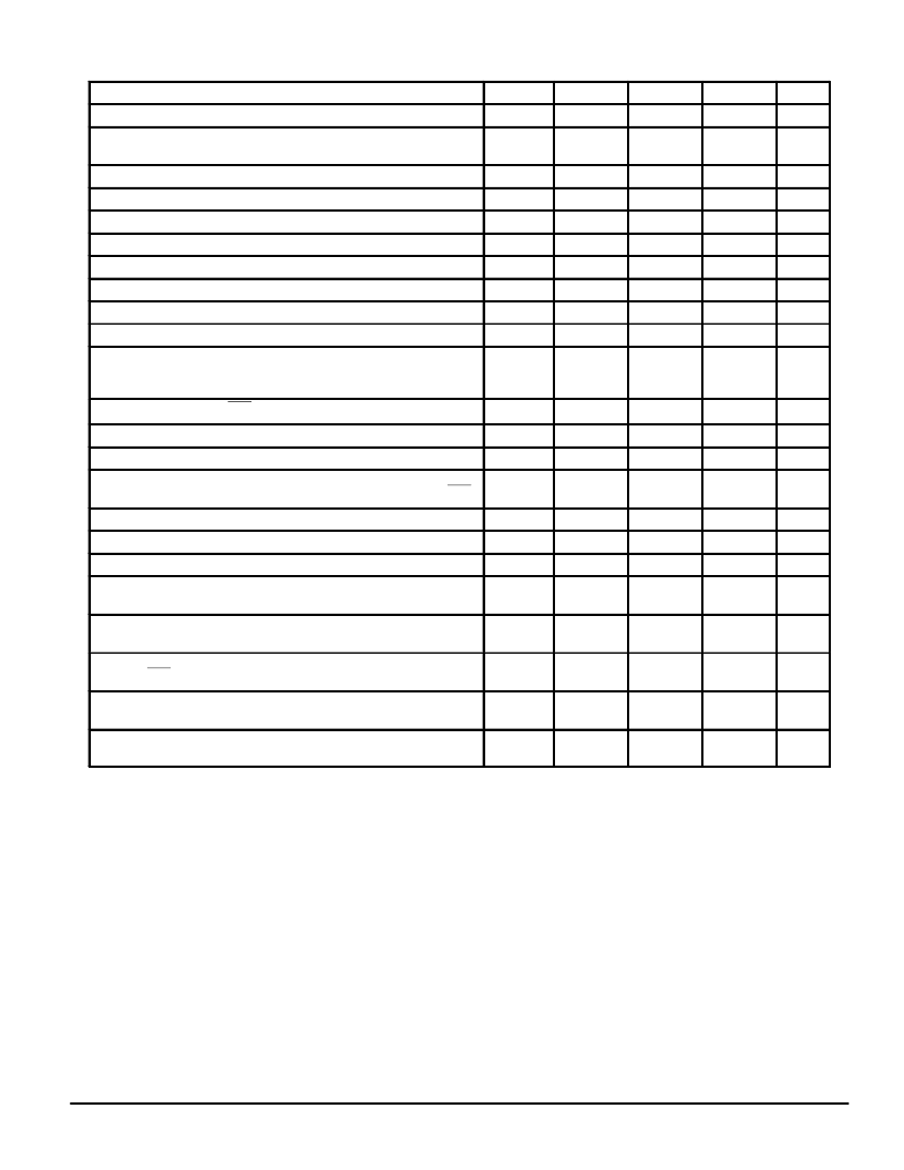
ANALOG ELECTRICAL CHARACTERISTICS
(VDD = – VSS = 5 V to 6 V
±
5%, TA = – 40 to + 85
°
C)
Characteristic
Symbol
Min
Typ
Max
Unit
Input Current
+Tx, –Tx (Txl for MC145500)
Iin
Zin
—
±
0.01
±
0.2
μ
A
AC Input Impedance to VAG (1 kHz)
+Tx, –Tx
Txl for MC145500
5
0.1
10
0.2
—
—
M
Input Capacitance
+Tx, –Tx
—
—
10
pF
Input Offset Voltage of Txl Op Amp
—
<
±
30
—
mV
Input Common Mode Voltage Range
+Tx, –Tx
VICR
CMRR
VSS + 1.0
—
—
VDD – 2.0
—
V
Input Common Mode Rejection Ratio
+Tx, –Tx
70
dB
Txl Unity Gain Bandwidth
RL
≥
10 k
RL
≥
10 k
BWp
AVOL
—
1000
—
kHz
Txl Open Loop Gain
—
75
—
dB
Equivalent Input Noise (C–Message) Between +Tx and –Tx, at Txl
—
– 20
—
dBrnC0
Output Load Capacitance for Txl Op Amp
0
—
100
pF
Output Voltage Range Txl Op Amp, RxO or RxO
RL = 10 k
to VAG
RL = 600
to VAG
Vout
VSS + 0.8
VSS + 1.5
±
5.5
—
—
VDD – 1.0
VDD – 1.5
V
Output Current Txl, RxO, RxO
VSS + 1.5 V
≤
Vout
≤
VDD – 1.5 V
—
—
mA
Output Impedance RxO, RxO*
0 to 3.4 kHz
Zout
—
3
—
Output Load Capacitance for RxO and RxO*
0
—
200
pF
Output dc Offset Voltage Referenced to VAG Pin
RxO
RxO*
—
—
—
—
±
100
±
150
mV
Internal Gainsetting Resistors for RxG to RxO and RxO
62
100
225
k
External Reference Voltage Applied to Vref (Referenced to VAG)
Vref Input Current
VAG Output Bias Voltage
0.5
—
VDD – 1.0
20
V
—
—
μ
A
—
0.53 VDD +
0.47 VSS
—
V
VAG Output Current
Source
Sink
IVAG
0.4
10.0
—
—
0.8
—
mA
Output Leakage Current During Power Down for the Txl Op Amp, VAG,
RxO, and RxO
—
—
±
30
μ
A
Positive Power Supply Rejection Ratio,
0 – 100 kHz @ 250 mV, C–Message Weighting
Transmit
Receive
45
55
50
65
—
—
dBC
Negative Power Supply Rejection Ratio,
0 – 100 kHz @ 250 mV, C–Message Weighting
Transmit
Receive
50
50
55
60
—
—
dBC
* Assumes that RxG is not connected for gain modifications to RxO.
相關PDF資料 |
PDF描述 |
|---|---|
| MC145501L | PCM Codec-Filter Mono-Circuit |
| MC145502 | Single Channel (1.2V) SVS w/ Watchdog in 5/SOT23 5-SOT-23 -40 to 85 |
| MC145502FN | PCM Codec-Filter Mono-Circuit |
| MC145502L | Single Channel (1.8V) SVS w/ Watchdog in 5/SOT23 5-SOT-23 -40 to 85 |
| MC145502P | PCM Codec-Filter Mono-Circuit |
相關代理商/技術參數(shù) |
參數(shù)描述 |
|---|---|
| MC145502FNR2 | 制造商:Freescale Semiconductor 功能描述: |
| MC145502P | 制造商:Motorola Inc 功能描述: |
| MC145503DWR2 | 制造商:Rochester Electronics LLC 功能描述:- Bulk |
| MC145503P | 制造商:Rochester Electronics LLC 功能描述:PCM CODEC-FILTER - Bulk |
| MC145505DWR2 | 制造商:Rochester Electronics LLC 功能描述:- Bulk 制造商:Motorola Inc 功能描述: 制造商:MOTOROLA 功能描述: |
發(fā)布緊急采購,3分鐘左右您將得到回復。