- 您現(xiàn)在的位置:買賣IC網(wǎng) > PDF目錄379306 > MC145503 (Motorola, Inc.) Single Channel (1.8V) SVS w/ Watchdog in 5/SOT23 5-SOT-23 -40 to 85 PDF資料下載
參數(shù)資料
| 型號: | MC145503 |
| 廠商: | Motorola, Inc. |
| 英文描述: | Single Channel (1.8V) SVS w/ Watchdog in 5/SOT23 5-SOT-23 -40 to 85 |
| 中文描述: | PCM編解碼器過濾單電路 |
| 文件頁數(shù): | 4/28頁 |
| 文件大?。?/td> | 539K |
| 代理商: | MC145503 |
第1頁第2頁第3頁當前第4頁第5頁第6頁第7頁第8頁第9頁第10頁第11頁第12頁第13頁第14頁第15頁第16頁第17頁第18頁第19頁第20頁第21頁第22頁第23頁第24頁第25頁第26頁第27頁第28頁
MC145500
MC145501
MC145502
MC145503
MC145505
4
MOTOROLA
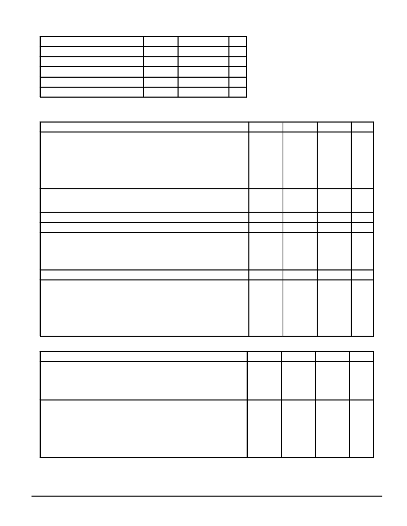
ABSOLUTE MAXIMUM RATINGS
(Voltage Referenced to VSS)
Rating
Symbol
Value
Unit
DC Supply Voltage
VDD, VSS
V
– 0.5 to 13
V
Voltage, Any Pin to VSS
DC Drain Per Pin (Excluding VDD, VSS)
Operating Temperature Range
– 0.5 to VDD + 0.5
10
V
I
mA
TA
Tstg
– 40 to + 85
°
C
Storage Temperature Range
– 85 to + 150
°
C
RECOMMENDED OPERATING CONDITIONS
(TA = – 40 to + 85
°
C)
Characteristic
Min
Typ
Max
Unit
DC Supply Voltage
Dual Supplies: VDD = – VSS, (VAG = VLS = 0 V)
Single Supply: VDD to VSS (VAG is an Output, VLS = VDD or VSS)
MC145500, MC145501, MC145502, MC145503, MC145505 (Using Internal
3.15 V Reference)
MC145501, MC145502 Using Internal 2.5 V Reference
MC145501, MC145502 Using Internal 3.78 V Reference
MC145502 Using External 1.5 V Reference, Referenced to VAG
4.75
8.5
7.0
9.5
4.75
5.0
—
—
—
—
6.3
12.6
12.6
12.6
12.6
V
Power Dissipation
CMOS Logic Mode (VDD to VSS = 10 V, VLS = VDD)
TTL Logic Mode (VDD = + 5 V, VSS = – 5 V, VLS = VAG = 0 V)
—
—
40
50
70
90
mW
Power Down Dissipation
—
0.1
1.0
mW
Frame Rate Transmit and Receive
7.5
8.0
8.5
kHz
Data Rate
MC145500, MC145501, MC145503
Must Use One of These Frequencies, Relative to MSI Frequency of 8 kHz
—
—
—
—
—
128
1536
1544
2048
2560
—
—
—
—
—
kHz
Data Rate for MC145502, MC145505
64
—
4096
kHz
Full Scale Analog Input and Output Level
MC145500, MC145503, MC145505
MC145501, MC145502 (Vref = VSS)
RSI = VDD
RSI = VSS
RSI = VAG
RSI = VDD
RSI = VSS
RSI = VAG
MC145502 Using an External Reference Voltage Applied at Vref Pin
—
—
—
—
—
—
—
3.15
3.78
3.15
2.5
1.51 x Vref
1.26 x Vref
Vref
—
—
—
—
—
—
—
Vp
DIGITAL LEVELS
(VSS to VDD = 4.75 V to 12.6 V, TA = – 40 to + 85
°
C)
Characteristic
Symbol
Min
Max
Unit
Input Voltage Levels (TDE, TDC, RCE, RDC, RDD, DC, MSI, CCI, PDI)
CMOS Mode (VLS = VDD, VSS is Digital Ground)
“0”
“1”
“0”
“1”
TTL Mode (VLS
≤
VDD – 4.0 V, VLS is Digital Ground)
VIL
VIH
VIL
VIH
—
0.7 x VDD
—
VLS + 2.0 V
0.3 x VDD
—
VLS + 0.8 V
—
V
Output Current for TDD (Transmit Digital Data)
CMOS Mode (VLS = VDD, VSS = 0 V and is Digital Ground)
(VDD = 5 V, Vout = 0.4 V)
(VDD = 10 V, Vout = 0.5 V)
(VDD = 5 V, Vout = 4.5 V)
(VDD = 10 V, Vout = 9.5 V)
(VOL = 0.4 V)
(VOH = 2.4 V)
TTL Mode (VLS
≤
VDD – 4.75 V, VLS = 0 V and is Digital Ground)
IOL
IOH
IOL
IOH
1.0
3.0
– 1.0
– 3.0
1.6
– 0.2
—
—
—
—
—
—
mA
This device contains circuitry to protect
against damage due to high static voltages or
electric fields; however, it is advised that
normal precautions be taken to avoid applica-
tion of any voltage higher than maximum rated
voltages to this high impedance circuit. For
proper operation it is recommended that Vin
and Vout be constrained to the range VSS
≤
(Vin
or Vout)
≤
VDD.
Unused inputs must always be tied to an
appropriate logic voltage level (e.g., VSS, VDD,
VLS, or VAG).
相關(guān)PDF資料 |
PDF描述 |
|---|---|
| MC145503DW | PCM Codec-Filter Mono-Circuit |
| MC145503L | Single Channel (1.5V) SVS with /MR in 5/SOT23 5-SOT-23 -40 to 85 |
| MC145503P | PCM Codec-Filter Mono-Circuit |
| MC145505 | Single Channel (1.5V) SVS with /MR in 5/SOT23 5-SOT-23 -40 to 85 |
| MC145505DW | PCM Codec-Filter Mono-Circuit |
相關(guān)代理商/技術(shù)參數(shù) |
參數(shù)描述 |
|---|---|
| MC145503DWR2 | 制造商:Rochester Electronics LLC 功能描述:- Bulk |
| MC145503P | 制造商:Rochester Electronics LLC 功能描述:PCM CODEC-FILTER - Bulk |
| MC145505DWR2 | 制造商:Rochester Electronics LLC 功能描述:- Bulk 制造商:Motorola Inc 功能描述: 制造商:MOTOROLA 功能描述: |
| MC145505P | 制造商:Rochester Electronics LLC 功能描述:PCM CODEC-FILTER - Bulk 制造商:Motorola Inc 功能描述: 制造商:MOTOROLA 功能描述: |
| MC145506P | 制造商:Rochester Electronics LLC 功能描述:LOW VOLTAGE COMPANDER - Bulk |
發(fā)布緊急采購,3分鐘左右您將得到回復(fù)。