- 您現(xiàn)在的位置:買賣IC網(wǎng) > PDF目錄371022 > MC33111 (Motorola, Inc.) Low Voltage Compander PDF資料下載
參數(shù)資料
| 型號: | MC33111 |
| 廠商: | Motorola, Inc. |
| 英文描述: | Low Voltage Compander |
| 中文描述: | 低電壓擴展器 |
| 文件頁數(shù): | 2/12頁 |
| 文件大小: | 131K |
| 代理商: | MC33111 |

MOTOROLA
2
MC33111
PIN FUNCTION DESCRIPTION
Name
Pin
Description
Ground
1
Connect to a clean power supply ground.
Compressor Output
2
Output of the compressor section.
Compressor input. The input impedance is nominally 10 k
. Nominal signal range is
1.0 mVrms to 1.0 Vrms in normal mode, and up to 0.8 Vrms in passthrough mode.
Must be capacitor coupled to the signal source.
Compressor Input
3
Compressor Mute
4
A logic high mutes the compressor. A logic low permits normal operation and passthrough.
Compressor Filter
5
Connect an external capacitor to filter the full wave rectifier’s output.
This capacitor affects attack and decay times, and low frequency accuracy.
Amplifier #1
6, 7
Inverting input (7) and output (6) of an op amp internally referenced to Vb.
Passthrough
8
A logic high sets the gain of both expander and compressor to
≈
0 dB, independent of
input level.
Amplifier #2
9, 10
Inverting input (9) and output (10) of an op amp internally referenced to Vb.
Expander Filter
11
Connect an external capacitor to filter the full wave rectifier’s output.
This capacitor affects attack and decay times, and low frequency accuracy.
Expander Mute
12
A logic high mutes the expander. A logic low permits normal operation and passthrough.
No Connect
13
This pin is not internally connected to anything.
Expander Input
14
Expander input. The input impedance is nominally 10.9 k
. Nominal signal range is
10 mVrms to 316 mVrms in normal mode, and up to 1.0 Vrms in passthrough mode.
Must be capacitor coupled to the signal source.
Expander Output
15
Output of the expander section.
VCC
16
Power supply. Connect to a power supply voltage in the range of 3.0 V to 7.0 V.
Bypass capacitor should be provided at this pin.
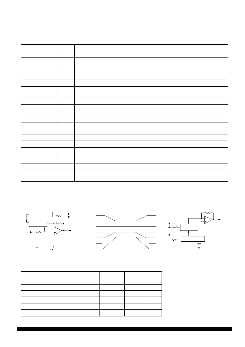
TRANSFER FUNCTIONS
Vb
15 k
Rectifier
40 k
Gain
Vout
Vin
Vout = 10 x Vin2
Expander
Compressor
Vb
Rectifier
Gain
Vin
Vout
10 k
Compression
Expansion
20 dB
10 dB
0 dB
–10 dB
– 20 dB
– 30 dB
– 40 dB
10 mV
31.6 mV
316 mV
1.0 V
100 mV
10 mV
1.0 mV
(Voltages are rms)
Vout
0.3162 x
Vin
MAXIMUM RATINGS
Rating
Symbol
Value
Unit
VCC Supply Voltage (Pin 16 – Pin 1)
High Input Voltage (Pins 3, 4, 8, 12, 14)
VCC
VIH
VIL
IO+
–0.5, +12
Vdc
VCC + 0.5
– 0.5
Vdc
Low Input Voltage (Pins 3, 4, 8, 12, 14)
Vdc
Output Source Current (Pins 2, 6, 10, 15)
Self-limiting
mA
Output Sink Current (Pins 2, 6, 10, 15)
IO–
Self-limiting
mA
Storage Temperature
Tstg
– 65, +150
°
C
NOTE:
Devices should not be operated at these limits. The “Recommended Operating Conditions”
provides for actual device operation.
相關PDF資料 |
PDF描述 |
|---|---|
| MC33128D | POWER MANAGEMENT CONTROLLER |
| MC33128 | POWER MANAGEMENT CONTROLLER |
| MC33143DW | DUAL HIGH-SIDE SWITCH |
| MC33143 | DUAL HIGH-SIDE SWITCH |
| MC33151D | HIGH SPEED DUAL MOSFET DRIVERS |
相關代理商/技術參數(shù) |
參數(shù)描述 |
|---|---|
| MC33111D | 制造商:FREESCALE 制造商全稱:Freescale Semiconductor, Inc 功能描述:Low Voltage Compander |
| MC33111P | 制造商:MOTOROLA 制造商全稱:Motorola, Inc 功能描述:LOW VOLTAGE COMPANDER |
| MC33121 | 制造商:MOTOROLA 制造商全稱:Motorola, Inc 功能描述:LOW VOLTAGE SUBSCRIBER LOOP INTERFACE CIRCUIT |
| MC33121FN | 制造商:Motorola Inc 功能描述: |
| MC33121P | 制造商:Rochester Electronics LLC 功能描述:SLIC III - Bulk |
發(fā)布緊急采購,3分鐘左右您將得到回復。