- 您現(xiàn)在的位置:買賣IC網(wǎng) > PDF目錄371022 > MC33111P (MOTOROLA INC) ECONOLINE: RSZ/P - 1kVDC PDF資料下載
參數(shù)資料
| 型號: | MC33111P |
| 廠商: | MOTOROLA INC |
| 元件分類: | 通信及網(wǎng)絡 |
| 英文描述: | ECONOLINE: RSZ/P - 1kVDC |
| 中文描述: | SPECIALTY TELECOM CIRCUIT, PDIP16 |
| 封裝: | PLASTIC, DIP-16 |
| 文件頁數(shù): | 9/12頁 |
| 文件大?。?/td> | 176K |
| 代理商: | MC33111P |

MOTOROLA
MC33111
9
40 k
Output
15
20 k
Gain
Rectifier
ICONTROL
Iref
11
Vb
15 k
VCC
14
Input
1.0
μ
F
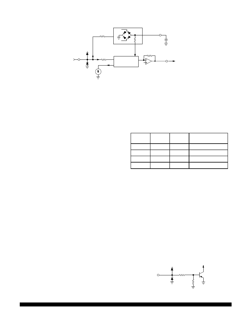
Figure 16. Expander
Expander
The expander is an noninverting amplifier with a fixed
feedback resistor and a variable gain cell in its input path as
shown in Figure 16.
The input signal is sampled by the precision rectifier which, in
turn, supplies a DC signal (ICONTROL), representative of the AC
input signal, to the variable gain cell. The reference current
(IREF) is an internally generated precision current. The effective
impedance of the variable gain cell varies with the ratio of the
two currents, and decreases as ICONTROL increases, thereby
providing expansion. The output is related to the input by the
following equation (Vin and Vout are rms volts):
Vout = 10 x (Vin)2
In terms of dB levels, the relationship is:
Vo(dB) = 2.0 x Vi(dB)
where 0 dB = 100 mVrms (See Figures 3 and 4).
The input and output are internally biased at Vb (
≈
+1.5 V),
and must therefore be capacitor coupled to external circuitry.
The input impedance at Pin 14 is nominally 10.9 k
(
±
20%),
and the maximum functional input signal is listed in the
Recommended Operating Conditions table. Bias currents
required by the op amp and the variable gain cell are
internally supplied. Due to clamp diodes at the input (to VCC
and ground), the input signal must be maintained between
the supply rails. If the input signal goes more than 0.5 V
above VCC or below ground, excessive currents will flow, and
distortion will show up at the output, and possibly in other
parts of the circuit.
The output of the rectifier is filtered by the capacitor at
Pin 11, which, in conjunction with an internal 20 k resistor,
provides the time constant for the attack and decay times.
The attack and decay times listed in the Electrical
Characteristics were determined using the test procedure
defined in EIA-553. Figure 10 indicates how the times vary
with the capacitor value. If the attack and decay times are
decreased by using a smaller capacitor, performance at low
frequencies will degrade.
(3)
(4)
Op Amps
The two op amps (at Pins 6, 7, 9, and 10) are identical and
can be used for peripheral functions, such as a microphone
amplifier, buffer, filter, etc. They have an open loop gain of
≈
100 dB, and a bandwidth of
≈
300 kHz. The noninverting
inputs are internally biased at Vb (
≈
+1.5 V). The inverting
inputs (Pins 7, 9) require a bias current of
≈
8.0 nA, which flows
into
the pin. The outputs can typically supply a maximum of 3.7
mA load current (see Electrical Characteristics).
NOTE
: If an op amp is unused, its output MUST be tied to
its input (Pin 6 to 7 and/or 9 to 10). Leaving an input open can
affect other portions of the IC.
Logic Inputs
The three inputs (Pins 4, 8, 12) provide for muting and
passthrough functions for the compressor and expander
according to the following truth table:
CM
(Pin 4)
EM
(Pin 12)
PT
(Pin 8)
Function
0
0
0
Normal Operation
1
X
X
Compressor Mute
X
1
X
Expander Mute
0
0
1
Passthrough
The logic section permits the compressor and expander to
be muted independently. The Passthrough control affects both
sections simultaneously, but only if the Mute inputs are at a logic
level 0. If both the Passthrough and a Mute input are asserted,
the Mute will override the Passthrough. The logic controls do
not affect the two uncommitted op amps in any way.
Figure 17 depicts a typical logic input stage configuration,
and Figure 14 indicates the typical input current. The inputs’
threshold is
≈
+1.3 V, independent of VCC. An open input is
equivalent to a logic low, but good design practices dictate
that inputs should never be left open. The inputs must be kept
within the range of VCC and GND. If an input is taken more
than 0.5 V above VCC or below GND excessive currents will
flow, and the device’s operation will be distorted.
Figure 17. Logic Input Stage
50 k
50 k
VCC
Pins
4, 8, 12
相關PDF資料 |
PDF描述 |
|---|---|
| MC33111 | Low Voltage Compander |
| MC33128D | POWER MANAGEMENT CONTROLLER |
| MC33128 | POWER MANAGEMENT CONTROLLER |
| MC33143DW | DUAL HIGH-SIDE SWITCH |
| MC33143 | DUAL HIGH-SIDE SWITCH |
相關代理商/技術參數(shù) |
參數(shù)描述 |
|---|---|
| MC33121 | 制造商:MOTOROLA 制造商全稱:Motorola, Inc 功能描述:LOW VOLTAGE SUBSCRIBER LOOP INTERFACE CIRCUIT |
| MC33121FN | 制造商:Motorola Inc 功能描述: |
| MC33121P | 制造商:Rochester Electronics LLC 功能描述:SLIC III - Bulk |
| MC33128 | 制造商:MOTOROLA 制造商全稱:Motorola, Inc 功能描述:POWER MANAGEMENT CONTROLLER |
| MC33128D | 制造商:MOTOROLA 制造商全稱:Motorola, Inc 功能描述:POWER MANAGEMENT CONTROLLER |
發(fā)布緊急采購,3分鐘左右您將得到回復。