- 您現(xiàn)在的位置:買賣IC網(wǎng) > PDF目錄371030 > MC33466H-33LT1 (MOTOROLA INC) FIXED FREQUENCY PWM MICROPOWER DC-to-DC CONVERTER PDF資料下載
參數(shù)資料
| 型號: | MC33466H-33LT1 |
| 廠商: | MOTOROLA INC |
| 元件分類: | 穩(wěn)壓器 |
| 英文描述: | FIXED FREQUENCY PWM MICROPOWER DC-to-DC CONVERTER |
| 中文描述: | SWITCHING CONTROLLER, 120 kHz SWITCHING FREQ-MAX, PSSO3 |
| 封裝: | PLASTIC, SOT-89, 3 PIN |
| 文件頁數(shù): | 7/12頁 |
| 文件大小: | 170K |
| 代理商: | MC33466H-33LT1 |

MC33466
7
MOTOROLA ANALOG IC DEVICE DATA
DEFINITIONS
Quiescent Bias Current
– Current which is used to operate
the switching regulator chip and is not delivered to the load.
Leakage Current
– Current drawn through a transistor
junction, under a specified collector voltage, when the
transistor is off.
FUNCTIONAL DESCRIPTION
Introduction
The MC33466 series are monolithic power switching
regulators optimized for dc–to–dc converter applications
where power drain must be minimized. The combination of
features in this series allows the system designer to directly
implement step–up, step–down or flyback converters with a
small number of external components. Potential applications
include low power consumer products and battery powered
portable products. Typical application circuits are shown in
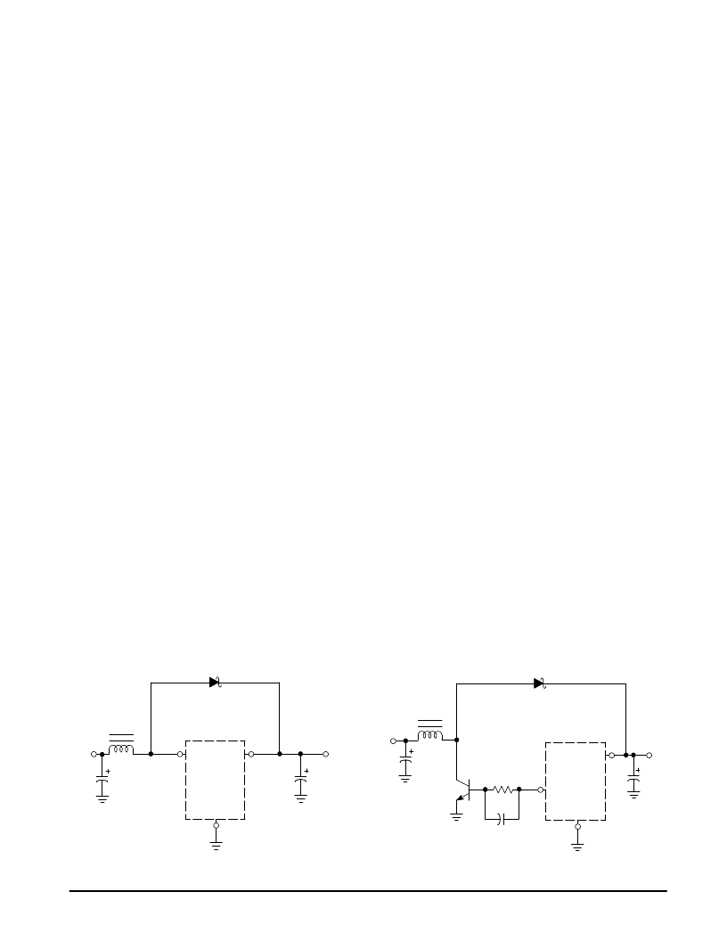
Figures 17 through 21.
Operating Description
The MC33466 series converters operate as a fixed
frequency voltage mode regulator. Operation is intended to
be in the discontinuous mode, where the inductor current
ramps up to a peak value which is greater than or equal to
twice the value of the dc input current during the on–time of
the transistor switch. During the off–time of the transistor
switch, the inductor current ramps down to zero and remains
at zero until another switching cycle begins.
Because the output voltage pin is also used as the supply
voltage for powering internal circuitry, an external startup
circuit is needed in step–down converter and flyback designs
to provide initial power to the integrated circuit to begin
switching. The startup circuit needed can be three discrete
components, as shown in Figure 19, or a micropower
undervoltage sensor, as shown in Figure 20.
Oscillator
The oscillator frequency, is internally programmed to
50 kHz. The timing capacitor (CT) discharge to charge ratio
of the oscillator is designed for a maximum duty cycle of 80%
at the Lx or EXT output. During the charge of CT, the
oscillator generates an internal blanking pulse that holds the
PWM control off, disabling the output transistor drive. The
oscillator peak and valley thresholds are 0.5 V and ground,
respectively.
Pulse Width Modulator
The Pulse Width Modulator consists of a comparator with
the oscillator ramp voltage applied to the inverting input,
while the error amplifier output is applied to the noninverting
input. Output switch conduction is initiated when the timing
capacitor is charged to its peak voltage value. When the
timing capacitor ramp discharges to a voltage below the error
amplifier output, the comparator resets a latch terminating
output transistor drive for the duration of the oscillator ramp
period.
Error Amplifier and Reference
An Error Amplifier is provided which has a nominal 80 dB
of voltage gain at dc. Internal compensation components
provide poles at 0.25 Hz, 30 kHz and 33 kHz. Two zeros are
provided at 1.0 kHz and at 2.5 kHz. The output voltage value
is set by the internal voltage divider and a 0.7 V reference
which is trimmed to an accuracy of
±
2.5%. Because the loop
compensation components are located within the IC,
discontinuous mode operation is recommended for most
applications.
Driver and Output Switch
To aid in system design flexibility and conversion
efficiency, two output driver options are provided. The
MC33466H–XXJT1 converters have an internal drive
transistor which is capable of sinking currents greater than
60 mA into the Lx pin. An internal VLx limiter circuit senses if
the Lx pin voltage exceeds 1.0 V during ton and turns off the
drive transistor. The MC33466H–XXJT1 provides output
drive for an external transistor.
Applications
The following converter applications show the simplicity
and flexibility of the converter architecture. Three main
converter topologies are demonstrated in Figures 17 through
21.
Figure 17. MC33466H–50KT1 Typical
Step–Up Application
MBRD520LT1
Vin
3
VO
Lx
Gnd
MC33466H–50KT1
22
μ
F
120
μ
H
1
VO
2
22
μ
F
Figure 18. MC33466H–50LT1 Typical
Step–Up Application
MBRD520LT1
Vin
3
MMBT2222ALT1
300
VO
EXT
Gnd
MC33466H–50LT1
100
μ
F
28
μ
H
0.01
μ
F
1
VO
5.0 V
2
22
μ
F
相關(guān)PDF資料 |
PDF描述 |
|---|---|
| MC33466H-50LT1 | FIXED FREQUENCY PWM MICROPOWER DC-to-DC CONVERTER |
| MC33466H-33JT1 | FIXED FREQUENCY PWM MICROPOWER DC-to-DC CONVERTER |
| MC33593 | PLL Tuned UHF Receiver for Data Transfer Applications |
| MC33593FTA | PLL Tuned UHF Receiver for Data Transfer Applications |
| MC3361B | Low Power Narrowband FM IF Receiver(低功耗窄帶FM IF接收器) |
相關(guān)代理商/技術(shù)參數(shù) |
參數(shù)描述 |
|---|---|
| MC33466H-50LT1 | 制造商:Rochester Electronics LLC 功能描述:- Bulk |
| MC3346D | 制造商:Rochester Electronics LLC 功能描述:- Bulk |
| MC3346DR2 | 制造商:Rochester Electronics LLC 功能描述:- Bulk |
| MC3346L | 制造商:Motorola Inc 功能描述:3346L |
| MC3346P | 制造商:Motorola Inc 功能描述: 制造商:Motorola Inc 功能描述:Bipolar Junction Transistor, Array, DIP |
發(fā)布緊急采購,3分鐘左右您將得到回復(fù)。