- 您現(xiàn)在的位置:買賣IC網 > PDF目錄379309 > MC3357D (MOTOROLA INC) Single Output LDO, 400mA, Fixed(3.3V), Low Noise, Fast Transient Response 8-MSOP -40 to 85 PDF資料下載
參數(shù)資料
| 型號: | MC3357D |
| 廠商: | MOTOROLA INC |
| 元件分類: | 接收器 |
| 英文描述: | Single Output LDO, 400mA, Fixed(3.3V), Low Noise, Fast Transient Response 8-MSOP -40 to 85 |
| 中文描述: | FM, AUDIO SINGLE CHIP RECEIVER, PDSO16 |
| 封裝: | PLASTIC, SO-16 |
| 文件頁數(shù): | 3/6頁 |
| 文件大?。?/td> | 123K |
| 代理商: | MC3357D |
MC3357
3
MOTOROLA ANALOG IC DEVICE DATA
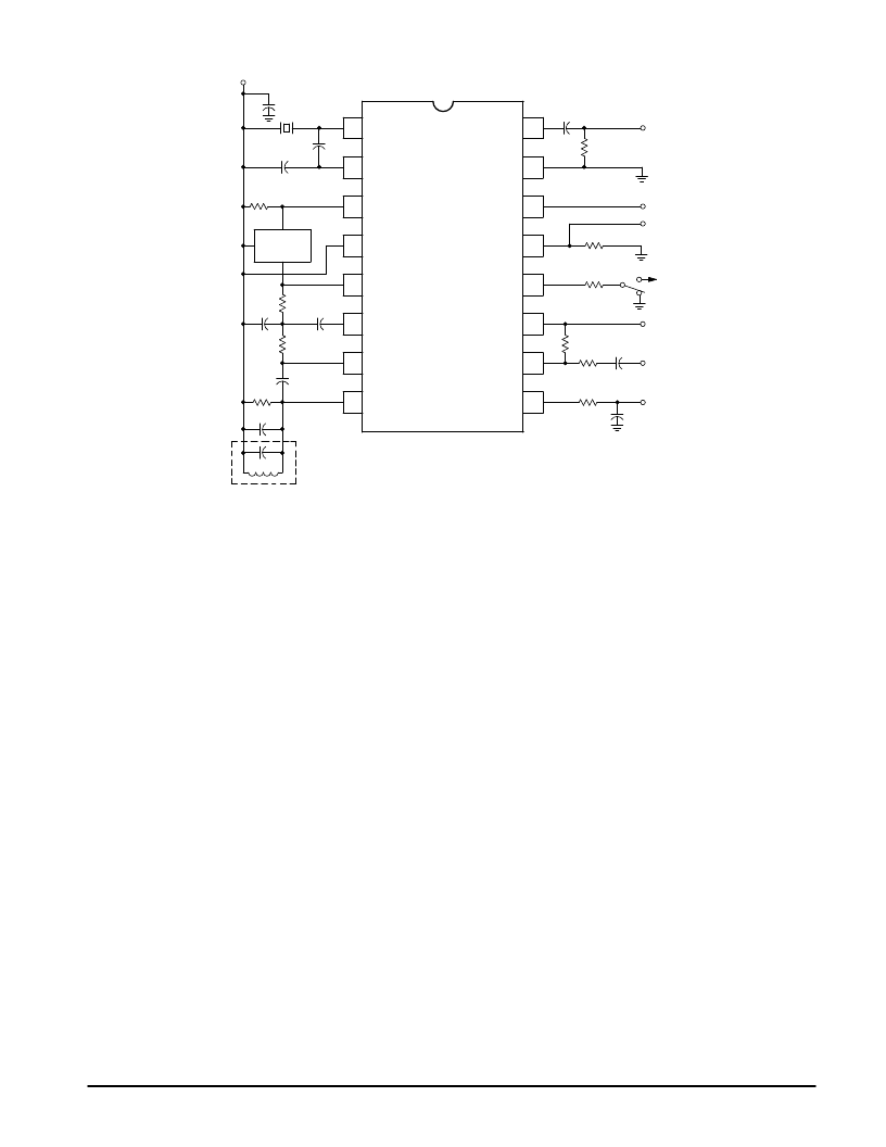
Figure 2. Test Circuit
20 pF
120 pF
0.1
μ
F
10.245 MHz
VCC = 6.0 Vdc
50 pF
2.0 k
455 kHz
Filter
100 nF
2.0 k
51 k
100 nF
47 k
10 pF
LP = 1.0 mH
CP = 100 pF
RP = 100 k
muRata
CFU
455 D
8.2 k
390 k
1.0 k
1.0
μ
F
+
Filter In
Audio Out
100 nF
10 k
10 k
51
Input
10.7 MHz
9
10
11
12
13
14
15
16
4
3
2
1
0.01
μ
F
2.0 Vdc
Op Amp Output
5
6
7
8
CIRCUIT DESCRIPTION
The MC3357 is a low power FM IF circuit designed
primarily for use in voice communication scanning receivers.
The mixer–oscillator combination converts the input
frequency (e.g., 10.7 MHz) down to 455 kHz, where, after
external bandpass filtering, most of the amplification is done.
The audio is recovered using a conventional quadrature FM
detector. The absence of an input signal is indicated by the
presence of noise above the desired audio frequencies. This
“noise band” is monitored by an active filter and a detector. A
squelch trigger circuit indicates the presence of a noise (or a
tone) by an output which can be used to control scanning. At
the same time, an internal switch is operated which can be
used to mute the audio.
The oscillator is an internally–biased Colpitts type with the
collector, base, and emitter connections at Pins 4, 1, and 2
respectively. A crystal can be used in place of the usual coil.
The mixer is doubly–balanced to reduce spurious
responses. The input impedance at Pin 16 is set by a 3.0 k
internal biasing resistor and has low capacitance, allowing
the circuit to be preceded by a crystal filter. The collector
output at Pin 3 must be dc connected to B +, below which it
can swing 0.5 V.
After suitable bandpass filtering (ceramic or LC), the signal
goes to the input of a five–stage limiter at Pin 5. The output of
the limiter at Pin 7 drives a multiplier, both internally directly,
and externally through a quadrature coil, to detect the FM. The
output at Pin 7 is also used to supply dc feedback to Pin 5. The
other side of the first limiter stage is decoupled at Pin 6.
The recovered audio is partially filtered, then buffered,
giving an impedance of around 400
at Pin 9. The signal still
requires de–emphasis, volume control and further
amplification before driving a loudspeaker.
A simple inverting op amp is provided with an output at Pin
11 providing dc bias (externally) to the input at Pin 10 which is
referred internally to 2.0 V. A filter can be made with external
impedance elements to discriminate between frequencies.
With an external AM detector, the filtered audio signal can be
checked for the presence of noise above the normal audio
band, or a tone signal. This information is applied to Pin 12.
An external positive bias to Pin 12 sets up the squelch
trigger circuit such that Pin 13 is low at an impedance level of
around 60 k
, and the audio mute (Pin 14) is open circuit. If
Pin 12 is pulled down to 0.7 V by the noise or tone detector,
Pin 13 will rise to approximately 0.5 Vdc below supply where
it can support a load current of around 500
μ
A and Pin 14 is
internally short–circuited to ground. There is 100 mV of
hysteresis at Pin 12 to prevent jitter. Audio muting is
accomplished by connecting Pin 14 to a high–impedance
ground–reference point in the audio path between Pin 9 and
the audio amplifier.
相關PDF資料 |
PDF描述 |
|---|---|
| MC3357P | Single Output LDO, 400mA, Fixed(3.3V), Low Noise, Fast Transient Response 8-MSOP -40 to 85 |
| MC3358P1 | DUAL DIFFERENTIAL INPUT OPERATIONAL AMPLIFIERS |
| MC3358P1 | DUAL DIFFERENTIAL INPUT OPERATIONAL AMPLIFIERS |
| MC3458P1 | DUAL DIFFERENTIAL INPUT OPERATIONAL AMPLIFIERS |
| MC3458 | DUAL DIFFERENTIAL INPUT OPERATIONAL AMPLIFIERS |
相關代理商/技術參數(shù) |
參數(shù)描述 |
|---|---|
| MC3357P | 制造商:Motorola Inc 功能描述: |
| MC33580BAPNA | 功能描述:電源開關 IC - 配電 QUAD 15MOHM HI SID RoHS:否 制造商:Exar 輸出端數(shù)量:1 開啟電阻(最大值):85 mOhms 開啟時間(最大值):400 us 關閉時間(最大值):20 us 工作電源電壓:3.2 V to 6.5 V 電源電流(最大值): 最大工作溫度:+ 85 C 安裝風格:SMD/SMT 封裝 / 箱體:SOT-23-5 |
| MC33580BAPNAR2 | 功能描述:電源開關 IC - 配電 QUAD 15MOHM HI SID RoHS:否 制造商:Exar 輸出端數(shù)量:1 開啟電阻(最大值):85 mOhms 開啟時間(最大值):400 us 關閉時間(最大值):20 us 工作電源電壓:3.2 V to 6.5 V 電源電流(最大值): 最大工作溫度:+ 85 C 安裝風格:SMD/SMT 封裝 / 箱體:SOT-23-5 |
| MC3358P1 | 制造商:Motorola 功能描述:3358 MOT'87 NOTES |
| MC33591FTA | 功能描述:射頻接收器 315 434 MHz RoHS:否 制造商:Skyworks Solutions, Inc. 類型:GPS Receiver 封裝 / 箱體:QFN-24 工作頻率:4.092 MHz 工作電源電壓:3.3 V 封裝:Reel |
發(fā)布緊急采購,3分鐘左右您將得到回復。