- 您現(xiàn)在的位置:買賣IC網(wǎng) > PDF目錄379310 > MC3479 (Motorola, Inc.) STEPPER MOTOR DRIVER PDF資料下載
參數(shù)資料
| 型號(hào): | MC3479 |
| 廠商: | Motorola, Inc. |
| 元件分類: | 基準(zhǔn)電壓源/電流源 |
| 英文描述: | STEPPER MOTOR DRIVER |
| 中文描述: | 步進(jìn)電機(jī)驅(qū)動(dòng)器 |
| 文件頁數(shù): | 2/10頁 |
| 文件大小: | 159K |
| 代理商: | MC3479 |
MC3479
2
MOTOROLA ANALOG IC DEVICE DATA
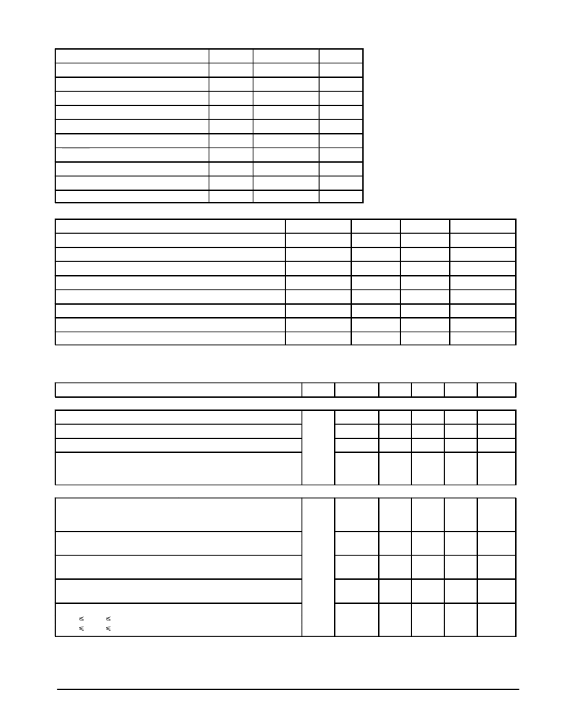
MAXIMUM RATINGS
Rating
Symbol
Value
Unit
Supply Voltage
VM
VD
VOD
IOD
Vin
IBS
VOA
IOA
TJ
Tstg
+ 18
Vdc
Clamp Diode Cathode Voltage (Pin 1)
VM + 5.0
VM + 6.0
±
500
Vdc
Driver Output Voltage
Vdc
Drive Output Current/Coil
mA
Input Voltage (Logic Controls)
– 0.5 to + 7.0
Vdc
Bias/Set Current
– 10
mA
Phase A Output Voltage
+ 18
Vdc
Phase A Sink Current
20
mA
Junction Temperature
+ 150
°
C
Storage Temperature Range
– 65 to + 150
°
C
RECOMMENDED OPERATING CONDITIONS
Characteristic
Symbol
Min
Max
Unit
Supply Voltage
VM
VD
IOD
Vin
IBS
VOA
IOA
TA
+ 7.2
+ 16.5
Vdc
Clamp Diode Cathode Voltage
VM
—
VM + 4.5
350
Vdc
Driver Output Current (Per Coil) (Note 1)
mA
Input Voltage (Logic Controls)
0
+ 5.5
Vdc
Bias/Set Current (Outputs Active)
– 300
– 75
μ
A
Phase A Output Voltage
—
VM
8.0
Vdc
Phase A Sink Current
0
mA
Operating Ambient Temperature
0
+ 70
°
C
NOTE:
1.
See section on Power Dissipation in Application Information.
DC ELECTRICAL CHARACTERISTICS
(Specifications apply over the recommended supply voltage and temperature range, [Notes
2, 3] unless otherwise noted.)
Characteristic
Pins
Symbol
Min
Typ
Max
Unit
INPUT LOGIC LEVELS
Threshold Voltage (Low–to–High)
7, 8,
9 10
9, 10
VTLH
VTHL
—
—
2.0
Vdc
Threshold Voltage (High–to–Low)
0.8
—
—
Vdc
Hysteresis
VHYS
IIL
0.4
—
—
Vdc
Current: (VI = 0.4 V)
Current:
(VI = 5.5 V)
Current:
(VI = 2.7 V)
–100
—
—
—
—
—
—
+100
+20
μ
A
DRIVER OUTPUT LEVELS
Output High Voltage
(IBS = – 300
μ
A): (IOD = – 350 mA)
(IBS = – 300
μ
A):
(IOD = – 0.1 mA)
2, 3,
14, 15
VOHD
Vdc
VM – 2.0
VM – 1.2
—
—
—
—
Output Low Voltage
(IBS = – 300
μ
A, IOD = 350 mA)
Differential Mode Output Voltage Difference (Note 4)
(IBS = – 300
μ
A, IOD = 350 mA)
Common Mode Output Voltage Difference (Note 5)
(IBS = – 300
μ
A, IOD = – 0.1 mA)
Output Leakage, Hi Z State
(0
VOD
VM, IBS = – 5.0
μ
A)
(0
VOD
VM, IBS = – 300
μ
A, F/H = 2.0 V, OIC = 0.8 V)
VOLD
—
—
0.8
Vdc
DVOD
—
—
0.15
Vdc
CVOD
—
—
0.15
Vdc
μ
A
IOZ1
IOZ2
– 100
– 100
—
—
+ 100
+ 100
NOTES:
2.Algebraic convention rather than absolute values is used to designate limit values.
3.Current into a pin is designated as positive. Current out of a pin is designated as negative.
4.DVOD =
VOD1,2 – VOD3,4
where: VOD1,2 = (VOHD1 – VOLD2) or (VOHD2 – VOLD1), and
VOD3,4 = (VOHD3 – VOLD4) or (VOHD4 – VOLD3).
5.CVOD =
VOHD1 – VOHD2
or
VOHD3 – VOHD4
.
相關(guān)PDF資料 |
PDF描述 |
|---|---|
| MC3479P | STEPPER MOTOR DRIVER |
| MC34923 | Full-Bridge PWM Motor Driver |
| MC34923DW | Full-Bridge PWM Motor Driver |
| MC34923R2 | Full-Bridge PWM Motor Driver |
| MC34C86 | ECONOLINE: RSZ/P - 1kVDC |
相關(guān)代理商/技術(shù)參數(shù) |
參數(shù)描述 |
|---|---|
| MC34791 | 制造商:SPC Multicomp 功能描述:CONNECTOR FPC 1.25MM 6WAY 制造商:SPC Multicomp 功能描述:CONNECTOR, FPC, 1.25MM, 6WAY |
| MC34793 | 制造商:SPC Multicomp 功能描述:CONNECTOR FPC 1.25MM 8WAY 制造商:SPC Multicomp 功能描述:CONNECTOR, FPC, 1.25MM, 8WAY |
| MC34795 | 制造商:SPC Multicomp 功能描述:CONNECTOR FPC 1.25MM 8WAY 制造商:SPC Multicomp 功能描述:CONNECTOR, FPC, 1.25MM, 8WAY |
| MC34797 | 制造商:SPC Multicomp 功能描述:CONNECTOR FPC 1.25MM 10WAY |
| MC34799 | 制造商:SPC Multicomp 功能描述:CONNECTOR FPC 1.25MM 10WAY 制造商:SPC Multicomp 功能描述:CONNECTOR, FPC, 1.25MM, 10WAY |
發(fā)布緊急采購,3分鐘左右您將得到回復(fù)。