- 您現(xiàn)在的位置:買賣IC網(wǎng) > PDF目錄369901 > MC44817BD (MOTOROLA INC) TV AND VCR PLL TUNING CIRCUITS WITH 1.3 GHz PRESCALER AND 3-WIRE BUS PDF資料下載
參數(shù)資料
| 型號: | MC44817BD |
| 廠商: | MOTOROLA INC |
| 元件分類: | XO, clock |
| 英文描述: | TV AND VCR PLL TUNING CIRCUITS WITH 1.3 GHz PRESCALER AND 3-WIRE BUS |
| 中文描述: | PLL FREQUENCY SYNTHESIZER, 1300 MHz, PDSO16 |
| 封裝: | PLASTIC, SO-16 |
| 文件頁數(shù): | 3/8頁 |
| 文件大小: | 159K |
| 代理商: | MC44817BD |
MC44817/17B
3
MOTOROLA ANALOG IC DEVICE DATA
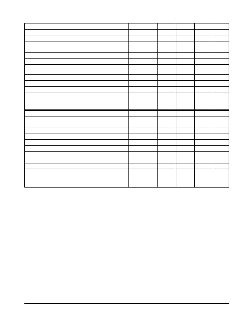
ELECTRICAL CHARACTERISTICS
(VCC1 = 5.0 V, VCC2 = 33 V, VCC3 = 12 V, TA = 25
°
C, unless otherwise noted.)
Characteristic
Pin
Min
Typ
Max
Unit
VCC1 Supply Voltage Range
VCC1 Supply Current (VCC1 = 5.0 V)
VCC2 Supply Voltage Range
VCC2 Supply Current (Output Open)
Band Buffer Leakage Current when “Off” at 12 V
7
4.5
5.0
5.5
V
7
–
37
50
mA
6
25
–
37
V
6
–
1.5
3.5
mA
10–13
–
0.01
1.0
μ
A
Band Buffer Saturation Voltage when “On” at 30 mA
10–13
–
0.15
0.3
V
Band Buffer Saturation Voltage when “On” at 40 mA
only for 0
°
to 80
°
C
10–13
–
0.2
0.5
V
Data/Clock/Enable Current at 0 V
1, 2, 16
–10
–
0
μ
A
μ
A
Data/Clock/Enable Current at 5.0 V
1, 2, 16
0
–
1.0
Data/Clock/Enable Input Voltage Low
1, 2, 16
–
–
1.5
V
Data/Clock/Enable Input Voltage High
1, 2, 16
3.0
–
–
V
Clock Frequency Range
2
–
–
100
kHz
Oscillator Frequency Range
3
3.15
3.2
4.05
MHz
Operational Amplifier Internal Reference Voltage
–
2.0
2.75
3.2
V
Operational Amplifier Input Current
4
–15
0
15
nA
DC Open Loop Voltage Gain
–
100
250
–
V/V
Gain Bandwidth Product (CL = 1.0 nF)
–
0.3
–
–
MHz
Vout Low, Sinking 50
μ
A
Vout High, Sourcing 10
μ
A, VCC2 – Vout
Phase Comparator Tri–State Current
5
–
0.2
0.4
V
5
–
0.2
0.5
V
4
–15
0
15
nA
Charge Pump High Current of Phase Comparator
4
30
50
85
μ
A
μ
A
Charge Pump Low Current of Phase Comparator
4
10
15
30
VCC3 Supply Voltage Range
VCC3 Supply Current
All Buffers “Off”
One Buffer “On” when Open
One Buffer “On” at 40 mA
14
VCC1
–
14.4
V
14
mA
–
–
–
0.2
8.0
48
0.5
13
53
Data Format and Bus Receiver
The circuit is controlled by a 3–wire bus via Data (DA),
Clock (CL), and Enable (EN) inputs. The Data and Clock
inputs may be shared with other inputs on the IIC–Bus while
the Enable is a separate signal. The circuit is compatible with
18 and 19 bit data transmission and also has a mode for
34 bit transmission for test and additional features.
The 3–wire bus receiver receives data for the internal shift
register after the positive going edge of the EN–signal. The
data is transmitted to the band buffers on the negative going
edge of the clock pulse 4 (signal DTB1).
18 and 19 Bit Data Transmission
The programmable divider may receive 14 bit (18 bit
transmission) or 15 bit (19 bit transmission). The data is
transmitted to the programmable divider (latches A) on the
negative going edge of clock pulse 19 or on the negative
edge of the EN–signal if EN goes down after the 18th clock
pulse (signal DTF). If the programmable divider receives
14 bit, its MSB (bit N14) is internally reset. The reset pulse is
generated only if EN goes negative after the 18th clock pulse
(signal RL).
34 Bit Data Transmission
(For Test and Additional Features)
In the test mode, the programmable divider receives 15 bit
and the data is transferred to latches A on the negative edge
of clock pulse 19 (signal DTF). The information for test is
received on clock pulses 20 to 26 and transmitted to the
latches on the negative edge of pulse 34 (signal DTB2).
These latches have a power–on reset. The power–on reset
sets the programmable divider to a counting ratio of 256 or
higher and resets the corresponding latches to the test bits
T0 to T6 (signal POR). The bus receiver is not disturbed if the
data format is wrong. Useless bits are ignored. If for example
the Enable signal goes low after the clock pulse 9, bits one to
four are accepted as valid buffer information and the other
bits are ignored. If more than 34 bits are received, bit 35 and
the following are ignored.
Lock Detector
The lock–detector output is low in lock. The output goes
immediately high when an unlock condition is detected. The
output goes low again when the loop is in lock during a
complete period of the reference frequency.
相關PDF資料 |
PDF描述 |
|---|---|
| MC44817D | RW-D Series - Econoline Regulated DC-DC Converters; Input Voltage (Vdc): 12V; Output Voltage (Vdc): 12V; Power: 2W; DIP24 Low Profile Package; Dual Ouputs from a Single Supply; 2:1 Wide Range Voltage Input; 3kVDC Isolation; UL94V-0 Package Material; Continuous Short Circuit Protection; Low profile 7mm Height; Approved for Medical Applications; Efficiency to 85% |
| MC44818D | TV AND VCR PLL TUNING CIRCUIT WITH 1.3 GHz PRESCALER AND I2C BUS |
| MC44818 | TV AND VCR PLL TUNING CIRCUIT WITH 1.3 GHz PRESCALER AND I2C BUS |
| MC44824D | RW-S Series - Econoline Regulated DC-DC Converters; Input Voltage (Vdc): 12V; Output Voltage (Vdc): 15V; Power: 2W; DIP24 Low Profile Miniature Package; 1kVDC Isolation; Feedback Regulated Output; 2:1 Wide Range Voltage Input; Continuous Short Circuit Protection; Less than 7mm Height; SMD Pinning Option; Efficiency to 87% |
| MC44825D | TV AND VCR PLL TUNING CIRCUITS WITH 1.3 GHz PRESCALER AND I2C BUS |
相關代理商/技術參數(shù) |
參數(shù)描述 |
|---|---|
| MC44817BDR2 | 制造商:Rochester Electronics LLC 功能描述:- Bulk 制造商:Motorola Inc 功能描述: 制造商:MOTOROLA 功能描述: |
| MC44817D | 制造商:MOTOROLA 制造商全稱:Motorola, Inc 功能描述:PLL Tuning Circuits with 3-Wire Bus |
| MC44818 | 制造商:MOTOROLA 制造商全稱:Motorola, Inc 功能描述:TV AND VCR PLL TUNING CIRCUIT WITH 1.3 GHz PRESCALER AND I2C BUS |
| MC44818D | 制造商:MOTOROLA 制造商全稱:Motorola, Inc 功能描述:TV AND VCR PLL TUNING CIRCUIT WITH 1.3 GHz PRESCALER AND I2C BUS |
| MC44818DR2 | 制造商:Rochester Electronics LLC 功能描述:- Bulk |
發(fā)布緊急采購,3分鐘左右您將得到回復。