- 您現(xiàn)在的位置:買賣IC網(wǎng) > PDF目錄369901 > MC44818 (Motorola, Inc.) TV AND VCR PLL TUNING CIRCUIT WITH 1.3 GHz PRESCALER AND I2C BUS PDF資料下載
參數(shù)資料
| 型號(hào): | MC44818 |
| 廠商: | Motorola, Inc. |
| 英文描述: | TV AND VCR PLL TUNING CIRCUIT WITH 1.3 GHz PRESCALER AND I2C BUS |
| 中文描述: | 電視機(jī)和錄像機(jī)鎖相環(huán)調(diào)諧電路與1.3 GHz的分頻器和I2C總線 |
| 文件頁(yè)數(shù): | 4/8頁(yè) |
| 文件大小: | 158K |
| 代理商: | MC44818 |
MC44818
4
MOTOROLA ANALOG IC DEVICE DATA
Figure 2 shows the five bytes of information that are
needed for circuit operation: there is the chip address, two
bytes of control and band information and two bytes of
frequency information.
After the chip address, two or four data bytes may be
received: if three data bytes are received the third data byte
is ignored.
If five or more data bytes are received the fifth and
following data bytes are ignored and the last acknowledge
pulse is sent at the end of the fourth data byte.
The first and the third data bytes contain a function bit
which allows the IC to distinguish between frequency
information and control plus band information.
Frequency information is preceeded by a Logic “0”. If the
function bit is Logic “1” the two following bytes contain control
and band information. The first data byte, shifted after the
chip address, may be byte CO or byte FM.
The two permissible bus protocols with five bytes are
shown in Figure 2.
Figure 2. Definition of Bytes
CA_Chip Address
1
1
0
0
0
0/1
0/1
0
ACK
ééééééééééééééééééééééé
ééééééééééééééééééééééé
CO_Information
BA_Band Information
ééééééééééééééééééééééé
ééééééééééééééééééééééé
FM_Frequency Information
FL_Frequency Information
N7
N6
N5
N4
N3
N2
N1
N0
ACK
CA_Chip Address
1
1
0
0
0
0/1
0/1
0
ACK
ééééééééééééééééééééééé
ééééééééééééééééééééééé
0
N14
N13
N12
N11
FM_Frequency Information
N10
N9
N8
ACK
FL_Frequency Information
N7
ééééééééééééééééééééé
ééééééééééééééééééééééé
1
T14
T13
T12
T11
N6
N5
N4
N3
N2
N1
N0
ACK
ééééééééééééééééééééééé
é
é
CO_Information
T10
T9
T8
ACK
BA_Band Information
X
X
X
X
B3
B2
B1
B0
ACK
Chip Address
The chip address is programmable by Pin 16 (AS –
Address Select).
AS – Pin 16
Address (HEX.)
Gnd to 0.1 VCC1
Open or 0.2 VCC1 to 0.3 VCC1
0.4 VCC1 to 0.7 VCC1
0.8 VCC1 to 1.1 VCC1
C0
C2
C4
C6
Bits B0, B1, B2, B3: Control the Band Buffers
B0, B1, B2, B3 = 0
B0, B1, B2, B3
= 1
Buffer “Off”
Buffer “On”
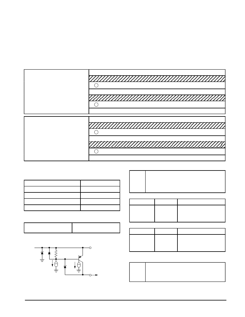
Figure 3. Equivalent Circuit of the Integrated
Band Buffers
“On”/“Off”
ISUB
30 mA (40 mA
at 0 to 80
°
C)
VCC3 12 V
25 V
Protection
IB
Out
B0
…
B3
NOTE:
IB + ISUB = 8.0 mA Typical, 13 mA Max
IB = Base Current
ISUB = Substrate Current of PNP
Gnd
Bit T8: Controls the Output of the Operational Amplifier
T8 = 0
Normal Operation
Operational Amplifier Active
Output State of Operational Amplifier Switched “Off”,
Output Pulls High Through 20 k Internal Pull–Up
Resistor
Bits T9, T12: Control the Phase Comparator
T9
T12
1
1
0
0
1
Bits T10, T11: Control the Reference Ratio
T10
T11
0
0
1
1
1
Bit T13: Switches the Internal Signals Fref and FBY2 to
Bit T13:
the Band Buffer Outputs (Test)
T13 = 0
T13
= 1
Test Mode
Fref Output at B2 (Pin 12)
FBY2 Output at B3 (Pin 13)
Bits B2 and B3 have to be “On”, B2 = B3 = 1 in the test mode.
Fref is the reference frequency.
FBY2 is the output frequency of the programmable divider, divided by two.
T8
= 1
Function
0
1
0
Normal Operation
High Impedance
Upper Source “On” Only
Lower Source “On” Only
Division Ratio
0
1
0
512
1024
1024
512
Normal Operation
相關(guān)PDF資料 |
PDF描述 |
|---|---|
| MC44824D | RW-S Series - Econoline Regulated DC-DC Converters; Input Voltage (Vdc): 12V; Output Voltage (Vdc): 15V; Power: 2W; DIP24 Low Profile Miniature Package; 1kVDC Isolation; Feedback Regulated Output; 2:1 Wide Range Voltage Input; Continuous Short Circuit Protection; Less than 7mm Height; SMD Pinning Option; Efficiency to 87% |
| MC44825D | TV AND VCR PLL TUNING CIRCUITS WITH 1.3 GHz PRESCALER AND I2C BUS |
| MC44826D | TV AND VCR I2C PLL TUNING CIRCUIT WITH 1.3 GHz PRESCALER AND MIX/OSC DECODER |
| MC44827BDTB | LOW-POWER PLL TUNING CIRCUIT |
| MC44827 | LOW-POWER PLL TUNING CIRCUIT |
相關(guān)代理商/技術(shù)參數(shù) |
參數(shù)描述 |
|---|---|
| MC44818D | 制造商:MOTOROLA 制造商全稱:Motorola, Inc 功能描述:TV AND VCR PLL TUNING CIRCUIT WITH 1.3 GHz PRESCALER AND I2C BUS |
| MC44818DR2 | 制造商:Rochester Electronics LLC 功能描述:- Bulk |
| MC44824D | 制造商:MOTOROLA 制造商全稱:Motorola, Inc 功能描述:TV AND VCR PLL TUNING CIRCUITS WITH 1.3 GHz PRESCALER AND I2C BUS |
| MC44825D | 制造商:MOTOROLA 制造商全稱:Motorola, Inc 功能描述:TV AND VCR PLL TUNING CIRCUITS WITH 1.3 GHz PRESCALER AND I2C BUS |
| MC44826D | 制造商:MOTOROLA 制造商全稱:Motorola, Inc 功能描述:TV AND VCR I2C PLL TUNING CIRCUIT WITH 1.3 GHz PRESCALER AND MIX/OSC DECODER |
發(fā)布緊急采購(gòu),3分鐘左右您將得到回復(fù)。