- 您現(xiàn)在的位置:買賣IC網(wǎng) > PDF目錄359147 > MC68HC908QC16 (飛思卡爾半導(dǎo)體(中國)有限公司) Microcontrollers PDF資料下載
參數(shù)資料
| 型號: | MC68HC908QC16 |
| 廠商: | 飛思卡爾半導(dǎo)體(中國)有限公司 |
| 英文描述: | Microcontrollers |
| 中文描述: | 微控制器 |
| 文件頁數(shù): | 238/274頁 |
| 文件大?。?/td> | 1782K |
| 代理商: | MC68HC908QC16 |
第1頁第2頁第3頁第4頁第5頁第6頁第7頁第8頁第9頁第10頁第11頁第12頁第13頁第14頁第15頁第16頁第17頁第18頁第19頁第20頁第21頁第22頁第23頁第24頁第25頁第26頁第27頁第28頁第29頁第30頁第31頁第32頁第33頁第34頁第35頁第36頁第37頁第38頁第39頁第40頁第41頁第42頁第43頁第44頁第45頁第46頁第47頁第48頁第49頁第50頁第51頁第52頁第53頁第54頁第55頁第56頁第57頁第58頁第59頁第60頁第61頁第62頁第63頁第64頁第65頁第66頁第67頁第68頁第69頁第70頁第71頁第72頁第73頁第74頁第75頁第76頁第77頁第78頁第79頁第80頁第81頁第82頁第83頁第84頁第85頁第86頁第87頁第88頁第89頁第90頁第91頁第92頁第93頁第94頁第95頁第96頁第97頁第98頁第99頁第100頁第101頁第102頁第103頁第104頁第105頁第106頁第107頁第108頁第109頁第110頁第111頁第112頁第113頁第114頁第115頁第116頁第117頁第118頁第119頁第120頁第121頁第122頁第123頁第124頁第125頁第126頁第127頁第128頁第129頁第130頁第131頁第132頁第133頁第134頁第135頁第136頁第137頁第138頁第139頁第140頁第141頁第142頁第143頁第144頁第145頁第146頁第147頁第148頁第149頁第150頁第151頁第152頁第153頁第154頁第155頁第156頁第157頁第158頁第159頁第160頁第161頁第162頁第163頁第164頁第165頁第166頁第167頁第168頁第169頁第170頁第171頁第172頁第173頁第174頁第175頁第176頁第177頁第178頁第179頁第180頁第181頁第182頁第183頁第184頁第185頁第186頁第187頁第188頁第189頁第190頁第191頁第192頁第193頁第194頁第195頁第196頁第197頁第198頁第199頁第200頁第201頁第202頁第203頁第204頁第205頁第206頁第207頁第208頁第209頁第210頁第211頁第212頁第213頁第214頁第215頁第216頁第217頁第218頁第219頁第220頁第221頁第222頁第223頁第224頁第225頁第226頁第227頁第228頁第229頁第230頁第231頁第232頁第233頁第234頁第235頁第236頁第237頁當(dāng)前第238頁第239頁第240頁第241頁第242頁第243頁第244頁第245頁第246頁第247頁第248頁第249頁第250頁第251頁第252頁第253頁第254頁第255頁第256頁第257頁第258頁第259頁第260頁第261頁第262頁第263頁第264頁第265頁第266頁第267頁第268頁第269頁第270頁第271頁第272頁第273頁第274頁
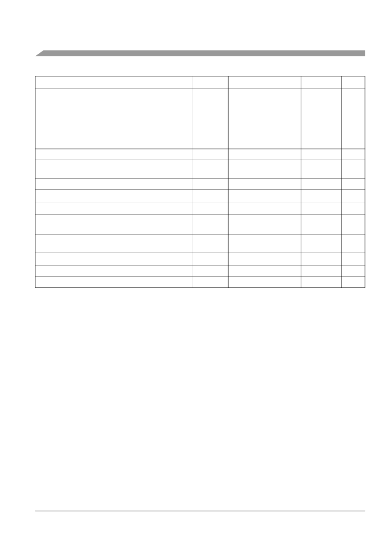
Electrical Specifications
MC68HC908QC16 MC68HC908QC8 MC68HC908QC4 Data Sheet, Rev. 2
238
Freescale Semiconductor
DC injection current
(3)
(4)
(5)
(6)
Single pin limit
V
in
> V
DD
V
in
< V
SS
Total MCU limit, includes sum of all stressed pins
V
in
> V
DD
V
in
< V
SS
I
IC
0
0
0
0
—
—
—
—
2
–0.2
25
–5
mA
Ports Hi-Z leakage current
I
IL
0
—
±
1
μ
A
Capacitance
Ports (as input)
(3)
C
IN
—
—
8
pF
POR rearm voltage
V
POR
750
—
—
mV
POR rise time ramp rate
(3)(7)
R
POR
0.035
—
—
V/ms
Monitor mode entry voltage
(3)
V
TST
V
DD
+ 2.5
—
9.1
V
Pullup resistors
(8)
PTA0–PTA5, PTB0–PTB7, PTC3–PTC0, PTD7–PTD0
R
PU
16
26
36
k
Ω
Pulldown resistors
(6)
PTA0–PTA5
R
PD
16
26
36
k
Ω
Low-voltage inhibit reset, trip falling voltage
(9)
V
TRIPF
3.90
4.20
4.50
V
Low-voltage inhibit reset, trip rising voltage
V
TRIPR
4.00
4.30
4.60
V
Low-voltage inhibit reset/recover hysteresis
V
HYS
—
100
—
mV
1. V
DD
= 4.5 to 5.5 Vdc, V
SS
= 0 Vdc, T
A
= T
L
to T
H
, unless otherwise noted.
2. Typical values reflect average measurements at midpoint of voltage range, 25°C only. Typical values are for reference only
and are not tested in production.
3. Values are based on characterization results, not tested in production.
4. All functional non-supply pins are internally clamped to V
SS
and V
DD
.
5. Input must be current limited to the value specified. To determine the value of the required current-limiting resistor, calculate
resistance values for positive and negative clamp voltages, then use the larger of the two values.
6. Power supply must maintain regulation within operating V
DD
range during instantaneous and operating maximum current
conditions. If positive injection current (V
in
> V
DD
) is greater than I
DD
, the injection current may flow out of V
DD
and could
result in external power supply going out of regulation. Ensure external V
DD
load will shunt current greater than maximum
injection current. This will be the greatest risk when the MCU is not consuming power. Examples are: if no system clock is
present, or if clock rate is very low (which would reduce overall power consumption).
7. If minimum V
DD
is not reached before the internal POR reset is released, the LVI will hold the part in reset until minimum
V
DD
is reached.
8. R
PU
and R
PD,
is measured at
V
DD
= 5.0 V. Pulldown resistors only available when KBIx is enabled with KBIxPOL =1.
9. Functionality of MCU guaranteed by production test down to minimum LVI trip point. The electrical parameters are only
guaranteed within the specified operating voltage range.
Characteristic
(1)
Symbol
Min
Typ
(2)
Max
Unit
發(fā)布緊急采購,3分鐘左右您將得到回復(fù)。