- 您現(xiàn)在的位置:買(mǎi)賣(mài)IC網(wǎng) > PDF目錄26803 > MC74ACT74DR2 (MOTOROLA INC) ACT SERIES, DUAL POSITIVE EDGE TRIGGERED D FLIP-FLOP, COMPLEMENTARY OUTPUT, PDSO14 PDF資料下載
參數(shù)資料
| 型號(hào): | MC74ACT74DR2 |
| 廠(chǎng)商: | MOTOROLA INC |
| 元件分類(lèi): | 鎖存器 |
| 英文描述: | ACT SERIES, DUAL POSITIVE EDGE TRIGGERED D FLIP-FLOP, COMPLEMENTARY OUTPUT, PDSO14 |
| 封裝: | PLASTIC, SOIC-14 |
| 文件頁(yè)數(shù): | 2/6頁(yè) |
| 文件大?。?/td> | 188K |
| 代理商: | MC74ACT74DR2 |
MC74AC74 MC74ACT74
5-2
FACT DATA
SD
D
CP
CD
Q
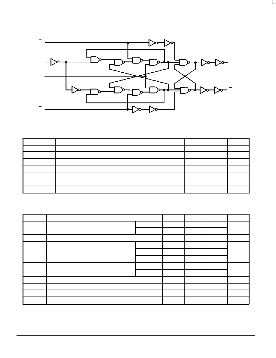
LOGIC DIAGRAM
Please note that this diagram is provided only for the understanding of logic
operations and should not be used to estimate propagation delays.
MAXIMUM RATINGS*
Symbol
Parameter
Value
Unit
VCC
DC Supply Voltage (Referenced to GND)
–0.5 to +7.0
V
Vin
DC Input Voltage (Referenced to GND)
–0.5 to VCC +0.5
V
Vout
DC Output Voltage (Referenced to GND)
–0.5 to VCC +0.5
V
Iin
DC Input Current, per Pin
±20
mA
Iout
DC Output Sink/Source Current, per Pin
±50
mA
ICC
DC VCC or GND Current per Output Pin
±50
mA
Tstg
Storage Temperature
–65 to +150
°C
* Maximum Ratings are those values beyond which damage to the device may occur. Functional operation should be restricted to the Recommended
Operating Conditions.
RECOMMENDED OPERATING CONDITIONS
Symbol
Parameter
Min
Typ
Max
Unit
VCC
Supply Voltage
′AC
2.0
5.0
6.0
V
VCC
Supply Voltage
′ACT
4.5
5.0
5.5
V
Vin, Vout
DC Input Voltage, Output Voltage (Ref. to GND)
0
VCC
V
tr, tf
Input Rise and Fall Time (Note 1)
′AC Devices except Schmitt Inputs
VCC @ 3.0 V
150
tr, tf
Input Rise and Fall Time (Note 1)
′AC Devices except Schmitt Inputs
VCC @ 4.5 V
40
ns/V
r, tf
′AC Devices except Schmitt Inputs
VCC @ 5.5 V
25
tr, tf
Input Rise and Fall Time (Note 2)
′ACT Devices except Schmitt Inputs
VCC @ 4.5 V
10
ns/V
tr, tf
Input Rise and Fall Time (Note 2)
′ACT Devices except Schmitt Inputs
VCC @ 5.5 V
8.0
ns/V
TJ
Junction Temperature (PDIP)
140
°C
TA
Operating Ambient Temperature Range
–40
25
85
°C
IOH
Output Current — High
–24
mA
IOL
Output Current — Low
24
mA
1. Vin from 30% to 70% VCC; see individual Data Sheets for devices that differ from the typical input rise and fall times.
2. Vin from 0.8 V to 2.0 V; see individual Data Sheets for devices that differ from the typical input rise and fall times.
相關(guān)PDF資料 |
PDF描述 |
|---|---|
| MC74AC74DR2 | AC SERIES, DUAL POSITIVE EDGE TRIGGERED D FLIP-FLOP, COMPLEMENTARY OUTPUT, PDSO14 |
| MC74ACT86M | ACT SERIES, QUAD 2-INPUT XOR GATE, PDSO14 |
| MC74ACT86DT | ACT SERIES, QUAD 2-INPUT XOR GATE, PDSO14 |
| MC74ACT86MR2 | ACT SERIES, QUAD 2-INPUT XOR GATE, PDSO14 |
| MC74F00JD | F/FAST SERIES, QUAD 2-INPUT NAND GATE, CDIP14 |
相關(guān)代理商/技術(shù)參數(shù) |
參數(shù)描述 |
|---|---|
| MC74ACT74DR2G | 功能描述:觸發(fā)器 5V CMOS Dual D-Type Positive Edge RoHS:否 制造商:Texas Instruments 電路數(shù)量:2 邏輯系列:SN74 邏輯類(lèi)型:D-Type Flip-Flop 極性:Inverting, Non-Inverting 輸入類(lèi)型:CMOS 輸出類(lèi)型: 傳播延遲時(shí)間:4.4 ns 高電平輸出電流:- 16 mA 低電平輸出電流:16 mA 電源電壓-最大:5.5 V 最大工作溫度:+ 85 C 安裝風(fēng)格:SMD/SMT 封裝 / 箱體:X2SON-8 封裝:Reel |
| MC74ACT74DR2G | 制造商:ON Semiconductor 功能描述:Standard Recovery Rectifier |
| MC74ACT74DT | 制造商:Rochester Electronics LLC 功能描述:- Bulk |
| MC74ACT74DTR2 | 功能描述:觸發(fā)器 5V CMOS Dual D-Type RoHS:否 制造商:Texas Instruments 電路數(shù)量:2 邏輯系列:SN74 邏輯類(lèi)型:D-Type Flip-Flop 極性:Inverting, Non-Inverting 輸入類(lèi)型:CMOS 輸出類(lèi)型: 傳播延遲時(shí)間:4.4 ns 高電平輸出電流:- 16 mA 低電平輸出電流:16 mA 電源電壓-最大:5.5 V 最大工作溫度:+ 85 C 安裝風(fēng)格:SMD/SMT 封裝 / 箱體:X2SON-8 封裝:Reel |
| MC74ACT74DTR2G | 功能描述:觸發(fā)器 5V CMOS Dual D-Type Positive Edge RoHS:否 制造商:Texas Instruments 電路數(shù)量:2 邏輯系列:SN74 邏輯類(lèi)型:D-Type Flip-Flop 極性:Inverting, Non-Inverting 輸入類(lèi)型:CMOS 輸出類(lèi)型: 傳播延遲時(shí)間:4.4 ns 高電平輸出電流:- 16 mA 低電平輸出電流:16 mA 電源電壓-最大:5.5 V 最大工作溫度:+ 85 C 安裝風(fēng)格:SMD/SMT 封裝 / 箱體:X2SON-8 封裝:Reel |
發(fā)布緊急采購(gòu),3分鐘左右您將得到回復(fù)。