- 您現(xiàn)在的位置:買賣IC網(wǎng) > PDF目錄371067 > MC74HC646N (MOTOROLA INC) Octal 3-State Bus Transeceivers and D Flip-Flops PDF資料下載
參數(shù)資料
| 型號(hào): | MC74HC646N |
| 廠商: | MOTOROLA INC |
| 元件分類: | 通用總線功能 |
| 英文描述: | Octal 3-State Bus Transeceivers and D Flip-Flops |
| 中文描述: | HC/UH SERIES, 8-BIT REGISTERED TRANSCEIVER, TRUE OUTPUT, PDIP24 |
| 封裝: | PLASTIC, DIP-24 |
| 文件頁數(shù): | 5/14頁 |
| 文件大小: | 328K |
| 代理商: | MC74HC646N |

MC54/74HC646
High–Speed CMOS Logic Data
DL129 — Rev 6
3–5
MOTOROLA
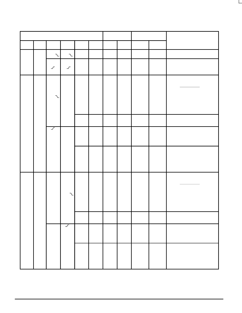
FUNCTION TABLE — HC646
Control Inputs
Data Port Status
Storage Flip–
Flop States
Description of Operation
Output
Enable
Direc–
tion
A–to–B
Clock
B–to–A
Clock
A–to–B
Source
B–to–A
Source
A
B
QA
QB
H
X
H, L,
H, L,
X
X
Input:
X
Input:
X
no change
no change
The output functions of the A and B
ports are disabled
X
X
L
H
X
X
X
X
L
H
L
H
X
X
X
X
L
H
The ports may be used as inputs to
the storage flip–flops. Data at the in-
puts are clocked into the flip–flops
with the rising edge of the Clocks.
L
H
Input:
Output:
The output mode of the B data port is
enabled and behaves according to
the following logic equation:
B = [A
(A–to–B Source)]
+ [Q
A
(A–to–B Source)]
1.) When A–to–B Source is low, the
data at the A data port are dis-
played at the B data port. The
states of the storage flip–flops are
not affected.
H, L,
X*
L
X
L
H
L
H
no change
no change
no change
no change
H
X
X
QA
no change
no change
2.) When A–to–B Source is high, the
states of the A storage flip–flops are
displayed at the B data port.
X*
L
X
L
H
L
H
L
H
no change
no change
3.) When A–to–B Source is low, the
data at the A data port are clocked
into the A storage flip–flops by a ris-
ing–edge signal on the A–to–B
Clock.
H
X
L
H
QA
QA
L
H
no change
no change
4.) When A–to–B Source is high, the
data at the A data port are clocked
into the A storage flip–flops by a ris-
ing–edge signal on the A–to–B
Clock. The states, QA, of the stor-
age flip–flops propagate directly to
the B data port.
L
L
Output:
Input:
The output mode of the A data port is
enabled and behaves according to
the following logic equation:
A = [B
(B–to–A Source)]
+ [Q
B
(B–to–A Source)]
1.) When B–to–A Source is low, the
data at the B data port are dis-
played at the A data port. The
states of the storage flip–flops are
not affected.
X*
H, L,
X
L
L
H
L
H
no change
no change
no change
no change
X
H
QB
X
no change
no change
2.) When B–to–A Source is high, the
states of the B storage flip–flops are
displayed at the A data port.
X*
X
L
L
H
L
H
no change
no change
L
H
3.) When B–to–A Source is low, the
data at the B data port are clocked
into the B storage flip–flops by a ris-
ing–edge signal on the B–to–A
Clock.
X
H
QB
QB
L
H
no change
no change
L
H
4.) When B–to–A Source is high, the
data at the B data port are clocked
into the B storage flip–flops by a ris-
ing–edge signal on the B–to–A
Clock. The states, QB, of the stor-
age flip–flops propagate directly to
the A data port.
* The clocks are not internally gated with either the Output Enables or the Source inputs. Therefore, data at the A and B ports may be clocked into
the storage flip–flops at any time.
相關(guān)PDF資料 |
PDF描述 |
|---|---|
| MC74HC7266A | SMPS Controller; Package: SOIC; No of Pins: 8; Container: Tape & Reel |
| MC74HC7266AD | SMPS Controller |
| MC74HC7266ADT | SMPS Controller |
| MC74HC7266AN | SMPS Controller |
| MC74HC7266D | Quad 2-Input Exclusive NOR Gate |
相關(guān)代理商/技術(shù)參數(shù) |
參數(shù)描述 |
|---|---|
| MC74HC688N | 制造商:ON Semiconductor 功能描述: |
| MC74HC7266AD | 制造商:ON Semiconductor 功能描述: |
| MC74HC7266AF | 制造商:Rochester Electronics LLC 功能描述:- Bulk |
| MC74HC7266AFEL | 制造商:Rochester Electronics LLC 功能描述:- Bulk |
| MC74HC7266AFR1 | 制造商:Rochester Electronics LLC 功能描述:- Bulk |
發(fā)布緊急采購,3分鐘左右您將得到回復(fù)。