- 您現(xiàn)在的位置:買賣IC網(wǎng) > PDF目錄26811 > MC88921DW (INTEGRATED DEVICE TECHNOLOGY INC) 88921 SERIES, PLL BASED CLOCK DRIVER, 5 TRUE OUTPUT(S), 0 INVERTED OUTPUT(S), PDSO20 PDF資料下載
參數(shù)資料
| 型號: | MC88921DW |
| 廠商: | INTEGRATED DEVICE TECHNOLOGY INC |
| 元件分類: | 時(shí)鐘及定時(shí) |
| 英文描述: | 88921 SERIES, PLL BASED CLOCK DRIVER, 5 TRUE OUTPUT(S), 0 INVERTED OUTPUT(S), PDSO20 |
| 封裝: | SOIC-20 |
| 文件頁數(shù): | 7/11頁 |
| 文件大?。?/td> | 544K |
| 代理商: | MC88921DW |
MC88921
TIMING SOLUTIONS
BR1333 — REV 5
5
MOTOROLA
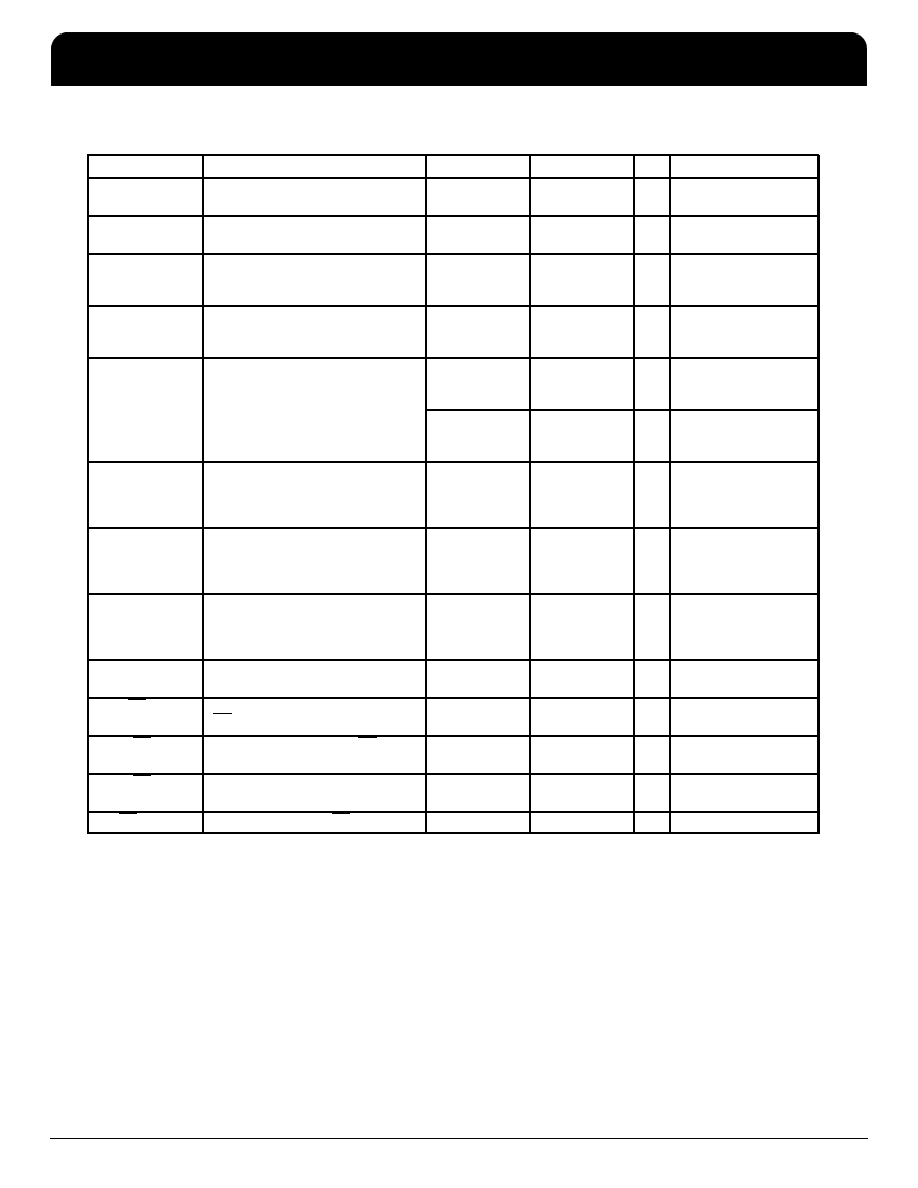
AC CHARACTERISTICS (TA = –40°C to 85°C; VCC = 5.0V ± 5%)
Symbol
Parameter
Minimum
Maximum
Unit
Condition
tRISE/FALL1
All Outputs
Rise/Fall Time, All Outputs into 50
Load
0.3
1.6
ns
tRISE – 0.8V to 2.0V
tFALL – 2.0V to 0.8V
tRISE/FALL1
2X_Q Output
Rise/Fall Time into a 20pF Load, With
Termination Specified in AppNote 3
0.5
1.6
ns
tRISE – 0.8V to 2.0V
tFALL – 2.0V to 0.8V
tpulse width(a)1
(Q0, Q1, Q2, Q3)
Output Pulse Width
Q0, Q1, Q2, Q3 at VCC/2
0.5tcycle – 0.55
0.5tcycle + 0.55
ns
50
Load Terminated to
VCC/2 (See Application
Note 3)
tpulse width(b)1
(2X_Q Output)
Output Pulse Width
2X_Q at VCC/2
0.5tcycle – 0.55
0.5tcycle + 0.55
ns
50
Load Terminated to
VCC/2 (See Application
Note 3)
tPD1,4
SYNC – Q/2
SYNC Input to Q Output Delay
(Measured at SYNC and Q/2 Pins)
–0.75
–0.15
ns
With 1M
From RC1
to An VCC
(See Application Note 2)
+1.25 7
+3.25 7
ns
With 1M
From RC1
to An GND
(See Application Note 2)
tSKEWr1,2
(Rising)
Output–to–Output Skew
Between Outputs Q0–Q3
(Rising Edge Only)
—
500
ps
Into a 50
Load
Terminated to VCC/2
(See Timing Diagram in
Figure 6)
tSKEWf1,2
(Falling)
Output–to–Output Skew
Between Outputs Q0–Q3
(Falling Edge Only)
—
1.0
ns
Into a 50
Load
Terminated to VCC/2
(See Timing Diagram in
Figure 6)
tSKEWall1,2
Output–to–Output Skew
2X_Q, Q0–Q3 Rising
—
1.0
ns
Into a 50
Load
Terminated to VCC/2
(See Timing Diagram in
Figure 6)
tLOCK3
Phase–Lock Acquisition Time,
All Outputs to SYNC Input
1
10
ms
tPHL MR – Q
Propagation Delay,
MR to Any Output (High–Low)
1.5
13.5
ns
Into a 50
Load
Terminated to VCC/2
tREC, MR to
SYNC6
Reset Recovery Time rising MR edge
to falling SYNC edge
9
—
ns
tREC, MR to
Normal Operation
Recovery Time for Outputs 2X_Q, Q0,
Q1 to Return to Normal PLL Operation
—
3 Clock Cycles
(Q Frequency)
ns
tW, MR LOW6
Minimum Pulse Width, MR input Low
5
—
ns
1. These specifications are not tested, they are guaranteed by statistical characterization. See Application Note 1 for a discussion of this
methodology.
2. Under equally loaded conditions and at a fixed temperature and voltage.
3. With VCC fully powered–on: tCLOCK Max is with C1 = 0.1F; tLOCK Min is with C1 = 0.01F.
4. See Application Note 4 for the distribution in time of each output referenced to SYNC.
5. Refer to Application Note 3 to translate signals to a 1.5V threshold.
6. Specification is valid only when the PLL_EN pin is low.
7. This is a typical specification only, worst case guarantees are not provided.
F
re
e
sc
a
le
S
e
m
ic
o
n
d
u
c
to
r,
I
Freescale Semiconductor, Inc.
For More Information On This Product,
Go to: www.freescale.com
n
c
..
.
MC88921
Low Skew CMOS PLL Clock Drivers With Power-Down/Power-up Feature
NETCOM
IDT Low Skew CMOS PLL Clock Drivers With Power-Down/Power-up Feature
Freescale Timing Solutions Organization has been acquired by Integrated Device Technology, Inc
MC88921
5
相關(guān)PDF資料 |
PDF描述 |
|---|---|
| MC88LV915TFN | 88LV SERIES, PLL BASED CLOCK DRIVER, 7 TRUE OUTPUT(S), 1 INVERTED OUTPUT(S), PQCC28 |
| MC88LV926DW | 88LV SERIES, PLL BASED CLOCK DRIVER, 4 TRUE OUTPUT(S), 1 INVERTED OUTPUT(S), PDSO20 |
| MD2FLDL-TTL-35G | ACTIVE DELAY LINE, TRUE OUTPUT, DSO6 |
| MD2FLDL-TTL-7F | ACTIVE DELAY LINE, TRUE OUTPUT, DIP6 |
| MD2FLDL-TTL-80G | ACTIVE DELAY LINE, TRUE OUTPUT, DSO6 |
相關(guān)代理商/技術(shù)參數(shù) |
參數(shù)描述 |
|---|---|
| MC889AL | 制造商:Rochester Electronics LLC 功能描述:- Bulk |
| MC889AP | 制造商:Motorola Inc 功能描述: 制造商:MOTOROLA 功能描述: |
| MC88A | 制造商:未知廠家 制造商全稱:未知廠家 功能描述:8 TUNES 8 KEY WITH SCAN KEY |
| MC88B/IVY | 制造商:TELEPHONE EQUIPMENT 功能描述:THREE COUPLER 8P8C |
| MC88I TERMINAL | 制造商:MC TECHNOLOGIES 功能描述:MOD GSM / GPRS QUADBAND TERMI 制造商:MC TECHNOLOGIES 功能描述:MOD, GSM / GPRS QUADBAND TERMINAL 制造商:MC TECHNOLOGIES 功能描述:MOD, GSM / GPRS QUADBAND TERMINAL; No. of Channels:4; Protocol:TCP / IP; Supply Voltage Min:8V; Supply Voltage Max:30V; Frequency RF:1.9GHz; Module Interface:RS232, USB; Kit Features:GPRS upto 86kbps, Data CSD upto 14.4kbps, Secure ;RoHS Compliant: Yes |
發(fā)布緊急采購,3分鐘左右您將得到回復(fù)。