- 您現(xiàn)在的位置:買賣IC網(wǎng) > PDF目錄45291 > MC9S08RE32CPE (FREESCALE SEMICONDUCTOR INC) 8-BIT, FLASH, 8 MHz, MICROCONTROLLER, PDIP28 PDF資料下載
參數(shù)資料
| 型號: | MC9S08RE32CPE |
| 廠商: | FREESCALE SEMICONDUCTOR INC |
| 元件分類: | 微控制器/微處理器 |
| 英文描述: | 8-BIT, FLASH, 8 MHz, MICROCONTROLLER, PDIP28 |
| 封裝: | ROHS COMPLIANT, PLASTIC, DIP-28 |
| 文件頁數(shù): | 78/234頁 |
| 文件大小: | 1758K |
| 代理商: | MC9S08RE32CPE |
第1頁第2頁第3頁第4頁第5頁第6頁第7頁第8頁第9頁第10頁第11頁第12頁第13頁第14頁第15頁第16頁第17頁第18頁第19頁第20頁第21頁第22頁第23頁第24頁第25頁第26頁第27頁第28頁第29頁第30頁第31頁第32頁第33頁第34頁第35頁第36頁第37頁第38頁第39頁第40頁第41頁第42頁第43頁第44頁第45頁第46頁第47頁第48頁第49頁第50頁第51頁第52頁第53頁第54頁第55頁第56頁第57頁第58頁第59頁第60頁第61頁第62頁第63頁第64頁第65頁第66頁第67頁第68頁第69頁第70頁第71頁第72頁第73頁第74頁第75頁第76頁第77頁當(dāng)前第78頁第79頁第80頁第81頁第82頁第83頁第84頁第85頁第86頁第87頁第88頁第89頁第90頁第91頁第92頁第93頁第94頁第95頁第96頁第97頁第98頁第99頁第100頁第101頁第102頁第103頁第104頁第105頁第106頁第107頁第108頁第109頁第110頁第111頁第112頁第113頁第114頁第115頁第116頁第117頁第118頁第119頁第120頁第121頁第122頁第123頁第124頁第125頁第126頁第127頁第128頁第129頁第130頁第131頁第132頁第133頁第134頁第135頁第136頁第137頁第138頁第139頁第140頁第141頁第142頁第143頁第144頁第145頁第146頁第147頁第148頁第149頁第150頁第151頁第152頁第153頁第154頁第155頁第156頁第157頁第158頁第159頁第160頁第161頁第162頁第163頁第164頁第165頁第166頁第167頁第168頁第169頁第170頁第171頁第172頁第173頁第174頁第175頁第176頁第177頁第178頁第179頁第180頁第181頁第182頁第183頁第184頁第185頁第186頁第187頁第188頁第189頁第190頁第191頁第192頁第193頁第194頁第195頁第196頁第197頁第198頁第199頁第200頁第201頁第202頁第203頁第204頁第205頁第206頁第207頁第208頁第209頁第210頁第211頁第212頁第213頁第214頁第215頁第216頁第217頁第218頁第219頁第220頁第221頁第222頁第223頁第224頁第225頁第226頁第227頁第228頁第229頁第230頁第231頁第232頁第233頁第234頁
Serial Peripheral Interface (SPI) Module
MC9S08RC/RD/RE/RG Data Sheet, Rev. 1.11
Freescale Semiconductor
169
When CPHA = 1, the slave begins to drive its MISO output when SS1 goes to active low, but the data is
not dened until the rst SPSCK edge. The rst SPSCK edge shifts the rst bit of data from the shifter
onto the MOSI output of the master and the MISO output of the slave. The next SPSCK edge causes both
the master and the slave to sample the data bit values on their MISO and MOSI inputs, respectively. At the
third SPSCK edge, the SPI shifter shifts one bit position which shifts in the bit value that was just sampled,
and shifts the second data bit value out the other end of the shifter to the MOSI and MISO outputs of the
master and slave, respectively. When CHPA = 1, the slave’s SS input is not required to go to its inactive
high level between transfers.
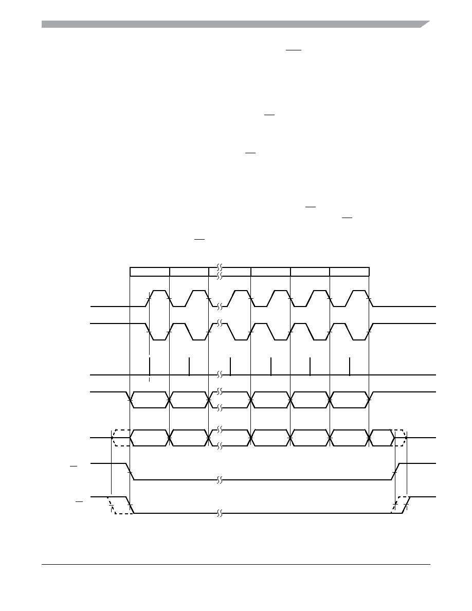
Figure 13-6 shows the clock formats when CPHA = 0. At the top of the gure, the eight bit times are shown
for reference with bit 1 starting as the slave is selected (SS IN goes low), and bit 8 ends at the last SPSCK
edge. The MSB rst and LSB rst lines show the order of SPI data bits depending on the setting in LSBFE.
Both variations of SPSCK polarity are shown, but only one of these waveforms applies for a specic
transfer, depending on the value in CPOL. The SAMPLE IN waveform applies to the MOSI input of a
slave or the MISO input of a master. The MOSI waveform applies to the MOSI output pin from a master
and the MISO waveform applies to the MISO output from a slave. The SS OUT waveform applies to the
slave select output from a master (provided MODFEN and SSOE = 1). The master SS output goes to active
low at the start of the rst bit time of the transfer and goes back high one-half SPSCK cycle after the end
of the eighth bit time of the transfer. The SS IN waveform applies to the slave select input of a slave.
Figure 13-6. SPI Clock Formats (CPHA = 0)
BIT TIME #
(REFERENCE)
MSB FIRST
LSB FIRST
SPSCK
(CPOL = 0)
SPSCK
(CPOL = 1)
SAMPLE IN
(MISO OR MOSI)
MOSI
(MASTER OUT)
MISO
(SLAVE OUT)
SS OUT
(MASTER)
SS IN
(SLAVE)
BIT 7
BIT 0
BIT 6
BIT 1
BIT 2
BIT 5
BIT 1
BIT 6
BIT 0
BIT 7
12
6
7
8
...
相關(guān)PDF資料 |
PDF描述 |
|---|---|
| MC9S08RD32CPE | 8-BIT, FLASH, 8 MHz, MICROCONTROLLER, PDIP28 |
| MC9S08RD60CPE | 8-BIT, FLASH, 8 MHz, MICROCONTROLLER, PDIP28 |
| MC9S08RE8FGE | 8-BIT, FLASH, 8 MHz, MICROCONTROLLER, PQFP44 |
| MC9S08RE32CFGE | 8-BIT, FLASH, 8 MHz, MICROCONTROLLER, PQFP44 |
| MC9S08RG60CFGE | 8-BIT, FLASH, 8 MHz, MICROCONTROLLER, PQFP44 |
相關(guān)代理商/技術(shù)參數(shù) |
參數(shù)描述 |
|---|---|
| MC9S08RE32DWE | 制造商:FREESCALE 制造商全稱:Freescale Semiconductor, Inc 功能描述:Microcontrollers |
| MC9S08RE32FDE | 制造商:FREESCALE 制造商全稱:Freescale Semiconductor, Inc 功能描述:Microcontrollers |
| MC9S08RE32FG | 制造商:MOTOROLA 制造商全稱:Motorola, Inc 功能描述:Microcontrollers |
| MC9S08RE32FGE | 制造商:FREESCALE 制造商全稱:Freescale Semiconductor, Inc 功能描述:Microcontrollers |
| MC9S08RE32FJ | 制造商:MOTOROLA 制造商全稱:Motorola, Inc 功能描述:Microcontrollers |
發(fā)布緊急采購,3分鐘左右您將得到回復(fù)。