- 您現(xiàn)在的位置:買賣IC網(wǎng) > PDF目錄369897 > MCC141511A (MOTOROLA INC) LCD Segment Driver CMOS PDF資料下載
參數(shù)資料
| 型號: | MCC141511A |
| 廠商: | MOTOROLA INC |
| 元件分類: | 顯示驅(qū)動器 |
| 英文描述: | LCD Segment Driver CMOS |
| 中文描述: | LIQUID CRYSTAL DISPLAY DRIVER, UUC159 |
| 封裝: | 0.1143 MM PITCH, DIE-159 |
| 文件頁數(shù): | 4/17頁 |
| 文件大小: | 292K |
| 代理商: | MCC141511A |
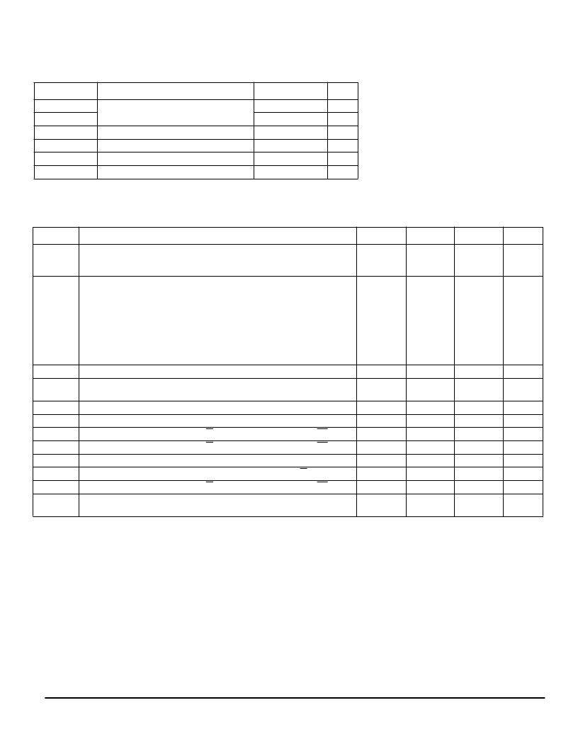
MOTOROLA
3–22
MC141511A
Symbol
Parameter
Value
Unit
V
DD
V
LCD
V
in
I
Supply Voltage
-0.3 to +7.0
V
-0.3 to +14.0
V
Input Voltage
V
SS
-0.3 to V
DD
+0.3
25
V
Current Drain Per Pin Excluding V
DD
and V
SS
Operating Temperature
mA
T
A
T
stg
-20 to +70
C
Storage Temperature Range
-65 to +150
C
MAXIMUM RATINGS*
(Voltages Referenced to V
SS
, T
A
= 25C)
* Maximum Ratings are those values beyond which damage to the device may occur. Functional
operation should be restricted to the limits in the Electrical Characteristics tables or Pin Description
section.
Symbol
Parameter
Min
Typ
Max
Unit
V
DD
V
LCD
Operating Voltage
Supply Voltage
LCD Voltage
2.7
4.5
-
-
5.5
13.2
V
V
I
AC
I
DP
I
SB
I
AC
I
DP
I
SB
I
LCD
V
OL
V
OH
V
OH
V
OL
V
IH
V
IL
V
R
I
in
C
in
I
OH
I
OL
Supply Current
at V
DD
=5.5V (PHI2=3.685MHz)
ACCESS
DISPLAY
STANDBY (Using D
ON
bit of the MCU)
at V
DD
=3.0V (PHI2=1.25MHz)
ACCESS
DISPLAY
STANDBY (Using D
ON
bit of the MCU)
Supply Current at V
LCD
Output Voltage, Iload210.0uA
-
-
-
-
-
-
-
25
15
-
17
10
200
30
20
200
30
20
uA
uA
uA
uA
uA
uA
-
-
200
uA
-
V
LCD
-0.1
V
DD
-0.8
-
-
0.1
-
V
V
Output High Voltage (Iload=1.6mA)
D7-D0
-
-
V
Output Low Voltage (Iload=1.6mA)
D7-D0
-
0.4
V
Input High Voltage
R/W, BPCLK, BPSYNC, PHI2, MS, CE, D7-D0
0.8xV
DD
V
SS
2.0
-
V
DD
V
Input Low Voltage
R/W, BPCLK, BPSYNC, PHI2, MS, CE, D7-D0
-
0.2xV
DD
-
V
Data Retention
-
V
Input Current
BPCLK, BPSYNC, R/W, PHI2, D7-D0
-
-
±1
uA
Capacitance
R/W, BPCLK, BPSYNC, PHI2, MS, CE, D7-D0
-
-
8
pF
Output current (V
OH
=4.5V, V
OL
=0.5V)
D7-D0
+20
-
-
-
-
-20
uA
uA
ELECTRICAL CHARACTERISTICS
(Voltage Referenced to V
SS
, T
A
= 25C)
This device contains circuitry to protect the inputs
against damage due to high static voltages or elec-
tric fields; however, it is advised that normal precau-
tions to be taken to avoid application of any voltage
higher than maximum rated voltages to this high
impedance circuit. For proper operation it is recom-
mended that V
in
and V
out
be constrained to the
range V
SS
< or = (V
in
or V
out
) < or = V
DD
. Reliability
of operation is enhanced if unused input are con-
nected to an appropriate logic voltage level (e.g.,
either V
SS
or V
DD
). Unused outputs must be left
open. This device may be light sensitive. Caution
should be taken to avoid exposure of this device to
any light source during normal operation. This
device is not radiation protected.
相關(guān)PDF資料 |
PDF描述 |
|---|---|
| MC141532 | LCD SEGMENT / COMMON DRIVER WITH CONTROLLER COMS |
| MC141533 | LCD SEGMENT / COMMON DRIVER WITH CONTROLLER COMS |
| MC141541P | Fixed-Point Digital Signal Processor 570-FCPGA -40 to 105 |
| MC141541 | Enhanced Monitor On-Screen Display |
| MC141543P | Floating Point Digital Signal Processor, Military 429-CFCBGA -55 to 115 |
相關(guān)代理商/技術(shù)參數(shù) |
參數(shù)描述 |
|---|---|
| MCC141531Z | 制造商:MOTOROLA 制造商全稱:Motorola, Inc 功能描述:LCD Segment/Common Driver CMOS |
| MCC141532Z | 制造商:MOTOROLA 制造商全稱:Motorola, Inc 功能描述:LCD Segment/Common Driver with Controller CMOS |
| MCC141533Z | 制造商:MOTOROLA 制造商全稱:Motorola, Inc 功能描述:LCD Segment/Common Driver with Controller CMOS |
| MCC141800AZ | 制造商:MOTOROLA 制造商全稱:Motorola, Inc 功能描述:LCD Segment/Common Driver |
| MCC1469 | 制造商:Rochester Electronics LLC 功能描述:- Bulk |
發(fā)布緊急采購,3分鐘左右您將得到回復(fù)。