- 您現(xiàn)在的位置:買賣IC網(wǎng) > PDF目錄371091 > MCM67C618FN9 (MOTOROLA INC) 64K x 18 Bit BurstRAM Synchronous Fast Static RAM PDF資料下載
參數(shù)資料
| 型號: | MCM67C618FN9 |
| 廠商: | MOTOROLA INC |
| 元件分類: | DRAM |
| 英文描述: | 64K x 18 Bit BurstRAM Synchronous Fast Static RAM |
| 中文描述: | 64K X 18 CACHE SRAM, 9 ns, PQCC52 |
| 封裝: | PLASTIC, LCC-52 |
| 文件頁數(shù): | 3/12頁 |
| 文件大?。?/td> | 214K |
| 代理商: | MCM67C618FN9 |
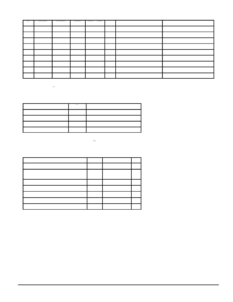
MCM67C518
3
MOTOROLA FAST SRAM
SYNCHRONOUS TRUTH TABLE
(See Notes 1, 2, and 3)
E
ADSP
ADSC
ADV
UW or LW
K
Address Used
Operation
H
L
X
X
X
L–H
N/A
Deselected
H
X
L
X
X
L–H
N/A
Deselected
L
L
X
X
X
L–H
External Address
Read Cycle, Begin Burst
L
H
L
X
L
L–H
External Address
Write Cycle, Begin Burst
L
H
L
X
H
L–H
External Address
Read Cycle, Begin Burst
X
H
H
L
L
L–H
Next Address
Write Cycle, Continue Burst
X
H
H
L
H
L–H
Next Address
Read Cycle, Continue Burst
X
H
H
H
L
L–H
Current Address
Write Cycle, Suspend Burst
X
H
H
H
H
L–H
Current Address
Read Cycle, Suspend Burst
NOTES:
1. X means Don’t Care.
2. All inputs except G must meet setup and hold times for the low–to–high transition of clock (K).
3. Wait states are inserted by suspending burst.
ASYNCHRONOUS TRUTH TABLE
(See Notes 1 and 2)
Operation
G
I/O Status
Read
L
Data Out
Read
H
High–Z
Write
X
High–Z — Data In
Deselected
X
High–Z
NOTES:
1. X means Don’t Care.
2. For a write operation following a read operation, G must be high before the input data
required setup time and held high through the input data hold time.
ABSOLUTE MAXIMUM RATINGS
(Voltages Referenced to VSS = 0 V)
Rating
Symbol
Value
Unit
Power Supply Voltage
VCC
– 0.5 to + 7.0
V
Voltage Relative to VSS for Any
Pin Except VCC
Vin, Vout
– 0.5 to VCC + 0.5
V
Output Current (per I/O)
Iout
±
30
mA
Power Dissipation
PD
1.6
W
Temperature Under Bias
Tbias
– 10 to + 85
°
C
Operating Temperature
TA
0 to +70
°
C
Storage Temperature
Tstg
– 55 to + 125
°
C
NOTE: Permanent device damage may occur if ABSOLUTE MAXIMUM RATINGS are
exceeded. Functional operation should be restricted to RECOMMENDED OPER-
ATING CONDITIONS. Exposure to higher than recommended voltages for
extended periods of time could affect device reliability.
This device contains circuitry to protect the
inputs against damage due to high static volt-
ages or electric fields; however, it is advised
that normal precautions be taken to avoid
application of any voltage higher than maxi-
mum rated voltages to this high–impedance
circuit.
This BiCMOS memory circuit has been
designed to meet the dc and ac specifications
shown in the tables, after thermal equilibrium
has been established.
This device contains circuitry that will
ensure the output devices are in High–Z at
power up.
相關(guān)PDF資料 |
PDF描述 |
|---|---|
| MCM67D709FN16 | 128K x 9 Bit Synchronous Dual I/O Fast Static RAM |
| MCM67D709FN20 | 128K x 9 Bit Synchronous Dual I/O Fast Static RAM |
| MCM67D709 | 128K x 9 Bit Synchronous Dual I/O Fast Static RAM |
| MCM67C518FN6 | 32K x 18 Bit BurstRAM Synchronous Fast Static RAM |
| MCM67C518FN7 | 32K x 18 Bit BurstRAM Synchronous Fast Static RAM |
相關(guān)代理商/技術(shù)參數(shù) |
參數(shù)描述 |
|---|---|
| MCM67D709 | 制造商:MOTOROLA 制造商全稱:Motorola, Inc 功能描述:128K x 9 Bit Synchronous Dual I/O Fast Static RAM |
| MCM67D709FN16 | 制造商:MOTOROLA 制造商全稱:Motorola, Inc 功能描述:128K x 9 Bit Synchronous Dual I/O Fast Static RAM |
| MCM67D709FN20 | 制造商:MOTOROLA 制造商全稱:Motorola, Inc 功能描述:128K x 9 Bit Synchronous Dual I/O Fast Static RAM |
| MCM67H518 | 制造商:MOTOROLA 制造商全稱:Motorola, Inc 功能描述:32K x 18 Bit BurstRAM Synchronous Fast Static RAM |
| MCM67H518FN10 | 制造商:MOTOROLA 制造商全稱:Motorola, Inc 功能描述:32K x 18 Bit BurstRAM Synchronous Fast Static RAM |
發(fā)布緊急采購,3分鐘左右您將得到回復。