- 您現(xiàn)在的位置:買賣IC網(wǎng) > PDF目錄383585 > MCP131X (Microchip Technology Inc.) Voltage Supervisor PDF資料下載
參數(shù)資料
| 型號: | MCP131X |
| 廠商: | Microchip Technology Inc. |
| 英文描述: | Voltage Supervisor |
| 中文描述: | 電壓監(jiān)控 |
| 文件頁數(shù): | 8/44頁 |
| 文件大小: | 924K |
| 代理商: | MCP131X |
第1頁第2頁第3頁第4頁第5頁第6頁第7頁當(dāng)前第8頁第9頁第10頁第11頁第12頁第13頁第14頁第15頁第16頁第17頁第18頁第19頁第20頁第21頁第22頁第23頁第24頁第25頁第26頁第27頁第28頁第29頁第30頁第31頁第32頁第33頁第34頁第35頁第36頁第37頁第38頁第39頁第40頁第41頁第42頁第43頁第44頁
MCP131X/2X
DS21985A-page 8
2005 Microchip Technology Inc.
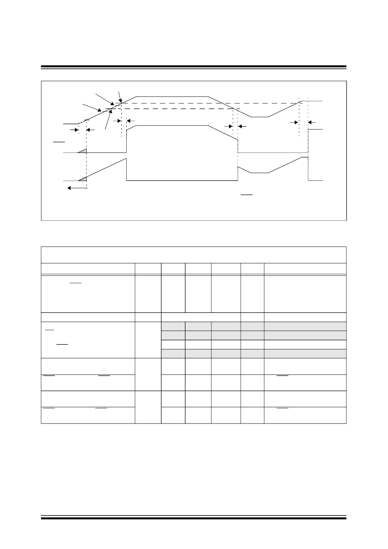
FIGURE 1-1:
Device Voltage and Reset Pin Waveforms.
TABLE 1-1:
Electrical Specifications:
Unless otherwise indicated, all limits are specified for V
DD
= 1V to 5.5V, R
PU
= 100 k
Ω
(only
MCP1320
,
MCP1321
and
MCP1322
), T
A
= -40°C to +125°C.
Parameters
Sym
Min
DEVICE VOLTAGE AND RESET PIN TIMINGS
Typ
Max
Units
Conditions
Falling V
DD
Trip Point Detected
to RST or RST Active
t
RPD
—
650
—
μ
s
V
DD
ramped from
V
TRIPMAX
+ 250 mV down to
V
TRIPMIN
– 200 mV,
V
DD
falling @ 5 mV/
μ
s,
C
L
= 50 pF
(Note 1)
V
DD
Rise Rate
Reset active time
(MR Rising Edge, POR/BOR
Inactive, or WDT time out) to
RST/RST Inactive
t
RR
t
RST
Note 3
1.4
30
200
1600
5
1.0
20
140
1120
—
2.0
40
280
2240
—
ms
ms
ms
ms
μ
s
Note 2
Note 2
Standard Time Out
Note 2
For RST 10% to 90% of V
DD
,
C
L
= 50 pF
(Note 1)
For RST 10% to 90% of V
DD
,
C
L
= 50 pF
(Note 1)
For RST 90% to 10% of V
DD
,
C
L
= 50 pF
(Note 1)
For RST 90% to 10% of V
DD
,
C
L
= 50 pF
(Note 1)
RST Rise Time After RST
Active
(Push-Pull Outputs only)
RST Rise Time After RST
Inactive
(Push-Pull Outputs only)
RST Fall Time after RST
Inactive
t
RT
—
5
—
μ
s
t
FT
—
5
—
μ
s
RST Fall Time after RST
Active
—
5
—
μ
s
Note 1:
These parameters are for design guidance only and are not 100% tested.
Custom ordered Reset active time; minimum order volume requirement.
Designed to be independent of V
DD
rise rate. Device characterization was done with a rise rate as slow as
0.1 V/s (@ +25°C).
2:
3:
V
TRIPMAX
V
TRIPMIN
V
TRIP
1V
V
DD
V
TRIPAC
+ V
HYS
t
RST
RST
RST
t
RR
t
RST
t
RPD
V
DD
< 1V is outside the device operating specification. The RST (or RST) output state is
unknown while V
DD
< 1V.
相關(guān)PDF資料 |
PDF描述 |
|---|---|
| MCP1320 | Voltage Supervisor |
| MCP1320T | Voltage Supervisor |
| MCP1321 | Voltage Supervisor |
| MCP1321T | Voltage Supervisor |
| MCP1322 | Voltage Supervisor |
相關(guān)代理商/技術(shù)參數(shù) |
參數(shù)描述 |
|---|---|
| MCP131X_12 | 制造商:MICROCHIP 制造商全稱:Microchip Technology 功能描述:Voltage Supervisor |
| MCP1320 | 制造商:MICROCHIP 制造商全稱:Microchip Technology 功能描述:Voltage Supervisor |
| MCP1320T | 制造商:MICROCHIP 制造商全稱:Microchip Technology 功能描述:Voltage Supervisor |
| MCP1320T-25LE | 制造商:MICROCHIP 制造商全稱:Microchip Technology 功能描述:Voltage Supervisor |
| MCP1320T-25LE/OT | 制造商:Microchip Technology Inc 功能描述: |
發(fā)布緊急采購,3分鐘左右您將得到回復(fù)。