- 您現(xiàn)在的位置:買賣IC網(wǎng) > PDF目錄1953 > MCP2021A-330E/MD (Microchip Technology)IC TXRX LIN 3.3V LDO 8-DFN PDF資料下載
參數(shù)資料
| 型號: | MCP2021A-330E/MD |
| 廠商: | Microchip Technology |
| 文件頁數(shù): | 46/48頁 |
| 文件大小: | 0K |
| 描述: | IC TXRX LIN 3.3V LDO 8-DFN |
| 產(chǎn)品培訓(xùn)模塊: | Microchip MCP20xx LIN Transceiver Overview |
| 標(biāo)準(zhǔn)包裝: | 91 |
| 系列: | * |
第1頁第2頁第3頁第4頁第5頁第6頁第7頁第8頁第9頁第10頁第11頁第12頁第13頁第14頁第15頁第16頁第17頁第18頁第19頁第20頁第21頁第22頁第23頁第24頁第25頁第26頁第27頁第28頁第29頁第30頁第31頁第32頁第33頁第34頁第35頁第36頁第37頁第38頁第39頁第40頁第41頁第42頁第43頁第44頁第45頁當(dāng)前第46頁第47頁第48頁

2012 Microchip Technology Inc.
DS22298A-page 7
MCP2021A/2A
Driving the TXD and checking the RXD pin make it
possible to determine whether there is a bus contention
(TXD = high, RXD = low) or a thermal overload
condition (TXD = low, RXD = high).
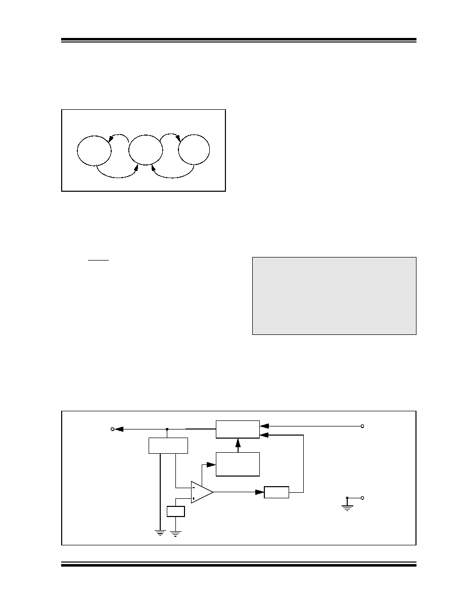
FIGURE 1-2:
THERMAL SHUTDOWN
STATE DIAGRAMS
1.3.3
TXD/LBUS TIME-OUT TIMER
The LIN bus can be driven to a dominant level either
from the TXD pin or externally. An internal timer deac-
tivates the LBUS transmitter if a dominant status
(LOW) on the LIN bus lasts longer than Bus Dominant
Time-out Time tTO(LIN) (approximately 20 milliseconds).
At the same time, RXD output is put in recessive
(HIGH), FAULT/TXE is also driven to LOW, and the
internal LIN pull-up resistor is disconnected. The timer
is reset on any recessive LBUS status or POR mode.
The recessive status on LBUS can be caused either by
the bus being externally pulled up or by the TXD pin
being returned high.
1.4
Internal Voltage Regulator
The MCP2021A/2A has a positive regulator capable of
supplying +5.00 or +3.30 VDC ±3% at up to 70 mA of
load current over the entire operating temperature
range of -40°C to +125°C. The regulator uses a LDO
design, is short-circuit-protected and will turn the regu-
lator output off if its output falls below the Shutdown
Voltage Threshold VSD.
With a load current of 70 mA, the minimum input to out-
put voltage differential required for the output to remain
in regulation is typically +0.5V (+1V maximum over the
full operating temperature range). Quiescent current is
less than 100 A with a full 70 mA load current when
the input to output voltage differential is greater than
+3.00V.
Regarding the correlation between VBB, VREG and IDD,
please refer to Figure 1-6 and Figure 1-7. When the
input voltage (VBB) drops below the differential needed
to provide stable regulation, the voltage regulator
output VREG will track the input down to approximately
VOFF. The regulator will turn off the output at this point.
This will allow PIC microcontrollers, with internal POR
circuits, to generate a clean arming of the Power-on
Reset trip point. The MCP2021A/2A will then monitor
VBB and turn on the regulator when VBB is above the
threshold of regulator turn on voltage VON.
In Power-down mode, the VBB monitor is turned off.
Under specific ambient temperature and battery
voltage range, the voltage regulator can output as high
as 150mA current. For current load capability of the
voltage regulator, refer Figure 1-4 and Figure 1-5.
The regulator requires an external output bypass
capacitor for stability. See Figure 2-1 for correct
capacity and ESR for stable operation.
FIGURE 1-3:
VOLTAGE REGULATOR BLOCK DIAGRAM
Operation
Mode
Transmitter
Shutdown
LIN bus
Voltage
Shutdown
Regulator
Output
Temp < SHUTDOWNTEMP
shorted
to VBB
Overload
Temp < SHUTDOWN
TEMP
Note:
The regulator overload current limit is
approximately 250 mA. The regulator out-
put voltage VREG is monitored. If output
voltage VREG is lower than VSD, the volt-
age regulator will turn off. After a recovery
time of about 3mS, the VREG will be
checked again. If there is no short circuit
(VREG > VSD), then the voltage regulator
remains on.
Pass
Element
Sampling
Network
Buffer
VREG
VBB
VSS
Fast
Transient
Loop
VREF
相關(guān)PDF資料 |
PDF描述 |
|---|---|
| MCP2022PT-500E/ST | IC TXRX LIN ON-BOARD VREG 14TSSO |
| MCP2022T-330E/ST | IC LIN TXRX ON-BD VREG 14TSSOP |
| MCP2036T-I/MG | INTEGRATED CIRCUITS LINEAR - 82 |
| MCP2036T-I/ML | IC AFE KEYLESS ENTRY 16QFN |
| MCP2050-500E/SL | IC TXRX LIN 5.0V LDO/WWDT 14SOIC |
相關(guān)代理商/技術(shù)參數(shù) |
參數(shù)描述 |
|---|---|
| MCP2021A-500E/MD | 功能描述:LIN 收發(fā)器 LIN Transceiver + 5.0V LDO RoHS:否 制造商:NXP Semiconductors 工作電源電壓: 電源電流: 最大工作溫度: 封裝 / 箱體:SO-8 |
| MCP2021A-500E/SN | 功能描述:LIN 收發(fā)器 LIN Transceiver + 5.0V LDO RoHS:否 制造商:NXP Semiconductors 工作電源電壓: 電源電流: 最大工作溫度: 封裝 / 箱體:SO-8 |
| MCP2021AT-330E/MD | 功能描述:LIN 收發(fā)器 LIN Transceiver + 3.3V LDO RoHS:否 制造商:NXP Semiconductors 工作電源電壓: 電源電流: 最大工作溫度: 封裝 / 箱體:SO-8 |
| MCP2021AT-330E/SN | 功能描述:LIN 收發(fā)器 LIN Transceiver + 3.3V LDO RoHS:否 制造商:NXP Semiconductors 工作電源電壓: 電源電流: 最大工作溫度: 封裝 / 箱體:SO-8 |
| MCP2021AT-500E/MD | 功能描述:LIN 收發(fā)器 LIN Transceiver + 5.0V LDO RoHS:否 制造商:NXP Semiconductors 工作電源電壓: 電源電流: 最大工作溫度: 封裝 / 箱體:SO-8 |
發(fā)布緊急采購,3分鐘左右您將得到回復(fù)。