- 您現(xiàn)在的位置:買賣IC網(wǎng) > PDF目錄1953 > MCP2022PT-500E/ST (Microchip Technology)IC TXRX LIN ON-BOARD VREG 14TSSO PDF資料下載
參數(shù)資料
| 型號: | MCP2022PT-500E/ST |
| 廠商: | Microchip Technology |
| 文件頁數(shù): | 8/52頁 |
| 文件大小: | 0K |
| 描述: | IC TXRX LIN ON-BOARD VREG 14TSSO |
| 產(chǎn)品培訓(xùn)模塊: | Microchip MCP20xx LIN Transceiver Overview |
| 標準包裝: | 2,500 |
| 系列: | * |
第1頁第2頁第3頁第4頁第5頁第6頁第7頁當前第8頁第9頁第10頁第11頁第12頁第13頁第14頁第15頁第16頁第17頁第18頁第19頁第20頁第21頁第22頁第23頁第24頁第25頁第26頁第27頁第28頁第29頁第30頁第31頁第32頁第33頁第34頁第35頁第36頁第37頁第38頁第39頁第40頁第41頁第42頁第43頁第44頁第45頁第46頁第47頁第48頁第49頁第50頁第51頁第52頁

MCP2021/2/1P/2P
DS22018F-page 16
2005-2012 Microchip Technology Inc.
1.6
Internal Voltage Regulator
1.6.1
5.0V REGULATOR
The MCP2021 has a low-drop-out voltage, positive reg-
ulator capable of supplying 5.00 VDC ±3% at up to
50 mA of load current over the entire operating temper-
ature range of -40°C to +125°C. With a load current of
50 mA, the minimum input to output voltage differential
required for the output to remain in regulation is typi-
cally +0.5V (+1V maximum over the full operating tem-
perature range). Quiescent current is less than 100 A
with a full 50 mA load current when the input to output
voltage differential is greater than +3.00V.
The regulator requires an external output bypass
capacitor for stability. See Figure 2-3 for correct
capacity and ESR for stable operation.
Designed for automotive applications, the regulator will
protect itself from double-battery jumps and up to +43V
load dump transients. The voltage regulator has both
short-circuit and thermal-shut-down protection built in.
Regarding the correlation between VBB, VREG and IDD,
please refer to Figure 1-10 throughFigure 1-12. When
the input voltage (VBB) drops below the differential
needed to provide stable regulation, the output VREG
will track the input down to approximately 3.5V, at
which point the regulator will turn off. This will allow
microcontrollers with internal POR circuits to generate
a clean arming of the POR trip point. The MCP2021 will
then monitor VBB and turn on the regulator when VBB
rises above 5.75, again.
When the input voltage (VBB) drops below the differen-
tial needed to provide stable regulation, the output
VREG) will track the input down to approximately
+4.25V. The regulator will turn off the output at this
point. This will allow PIC microcontrollers with internal
POR circuits to generate a clean arming of the POR trip
point. The regulator output will stay off until VBB is
above +5.75 VDC.
In the start phase, the device must detect at least 5.75V
to initiate operation during power up. In the Power-
Down mode, the VBB monitor will be turned off.
The regulator has a thermal shutdown. If the thermal
protection circuit detects an overtemperature condition,
and the signals TXD and RXD are LOW, or TXD is HIGH,
the regulator will shut down. The recovery from the
thermal shutdown is equal to adequate cooling time.
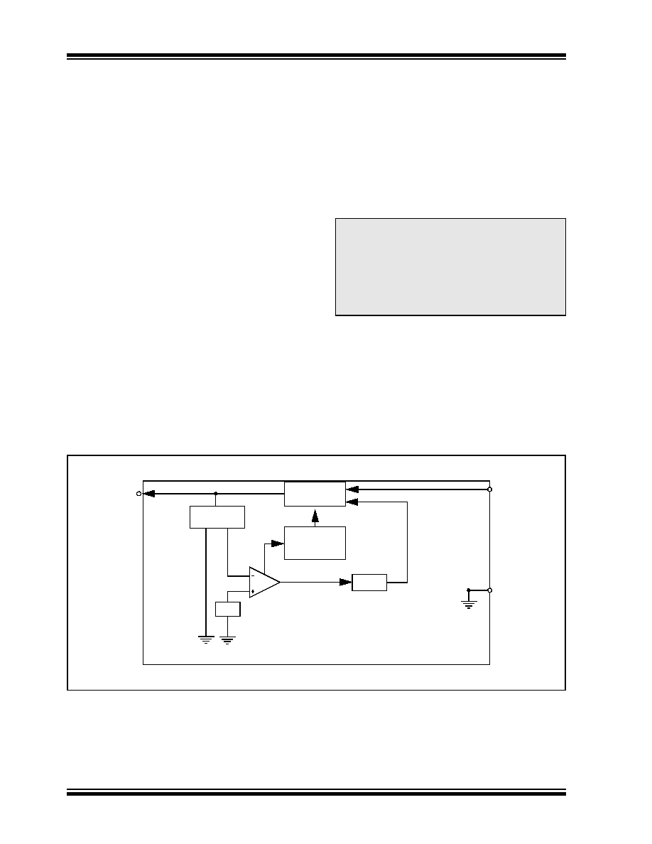
FIGURE 1-9:
Voltage Regulator Block Diagram.
Note:
The regulator has an overload current
limiting of approximately 100 mA. During a
short circuit, the VREG is monitored. If
VREG is lower than 3.5V, the VREG will turn
off. After a recovery time of about three
milliseconds, the VREG will be checked
again. If there is no short circuit (VREG
>3.5V), the VREG will be switched back on.
Pass
Element
Sampling
Network
Buffer
VREG
VBB
VSS
Fast
Transient
Loop
VREF
相關(guān)PDF資料 |
PDF描述 |
|---|---|
| MCP2022T-330E/ST | IC LIN TXRX ON-BD VREG 14TSSOP |
| MCP2036T-I/MG | INTEGRATED CIRCUITS LINEAR - 82 |
| MCP2036T-I/ML | IC AFE KEYLESS ENTRY 16QFN |
| MCP2050-500E/SL | IC TXRX LIN 5.0V LDO/WWDT 14SOIC |
| MCP2140-I/P | IC IRDA CONTROLLER DTE/DCE 18DIP |
相關(guān)代理商/技術(shù)參數(shù) |
參數(shù)描述 |
|---|---|
| MCP2022T | 制造商:MICROCHIP 制造商全稱:Microchip Technology 功能描述:LIN Transceiver with Voltage Regulator |
| MCP2022T-330E/MD | 制造商:MICROCHIP 制造商全稱:Microchip Technology 功能描述:LIN Transceiver with Voltage Regulator |
| MCP2022T-330E/MF | 制造商:MICROCHIP 制造商全稱:Microchip Technology 功能描述:LIN Transceiver with Voltage Regulator |
| MCP2022T-330E/P | 制造商:MICROCHIP 制造商全稱:Microchip Technology 功能描述:LIN Transceiver with Voltage Regulator |
| MCP2022T-330E/SL | 功能描述:LIN 收發(fā)器 LIN ver21 Trnsceivr 33V Vreg + RESET out RoHS:否 制造商:NXP Semiconductors 工作電源電壓: 電源電流: 最大工作溫度: 封裝 / 箱體:SO-8 |
發(fā)布緊急采購,3分鐘左右您將得到回復(fù)。