- 您現(xiàn)在的位置:買賣IC網(wǎng) > PDF目錄383590 > MCP455 (Microchip Technology Inc.) 400000 SYSTEM GATE 1.8 VOLT FPGA - NOT RECOMMENDED for NEW DESIGN PDF資料下載
參數(shù)資料
| 型號(hào): | MCP455 |
| 廠商: | Microchip Technology Inc. |
| 英文描述: | 400000 SYSTEM GATE 1.8 VOLT FPGA - NOT RECOMMENDED for NEW DESIGN |
| 中文描述: | 13.56 MHz讀/寫無源RFID器件 |
| 文件頁數(shù): | 7/50頁 |
| 文件大小: | 1172K |
| 代理商: | MCP455 |
第1頁第2頁第3頁第4頁第5頁第6頁當(dāng)前第7頁第8頁第9頁第10頁第11頁第12頁第13頁第14頁第15頁第16頁第17頁第18頁第19頁第20頁第21頁第22頁第23頁第24頁第25頁第26頁第27頁第28頁第29頁第30頁第31頁第32頁第33頁第34頁第35頁第36頁第37頁第38頁第39頁第40頁第41頁第42頁第43頁第44頁第45頁第46頁第47頁第48頁第49頁第50頁
2003 Microchip Technology Inc.
DS40232H-page 7
MCRF450/451/452/455
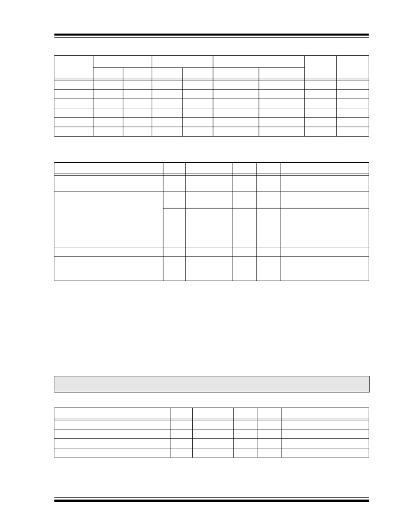
TABLE 2-4:
PAD COORDINATES (MICRONS)
TABLE 2-5:
DIE MECHANICAL DIMENSIONS
TABLE 2-6:
WAFER MECHANICAL SPECIFICATIONS
Pad Name
Lower
Upper
Passivation Openings
Pad
Center X
Pad
Center Y
Left X
Left Y
Right X
Right Y
Pad Width
Pad Height
Ant. Pad A
-853.50
-992.10
-764.50
-903.10
89.00
89.00
-809.00
-947.60
Ant. Pad B
759.50
-993.70
848.50
-904.70
89.00
89.00
804.00
-949.20
V
SS
769.10
977.90
858.10
1066.90
89.00
89.00
813.60
1022.40
V
DD
-839.50
45.50
-750.50
134.50
89.00
89.00
-795.00
90.00
CLK
721.10
77.80
810.10
166.80
89.00
89.00
765.60
122.30
F
CLK
-821.50
910.70
-732.50
999.70
89.00
89.00
-777.00
955.20
Note 1:
All coordinates are referenced from the center of the die.
Specifications
Min
Typ
Max
Unit
Comments
Bond pad opening
—
—
3.5 x 3.5
89 x 89
—
—
mil
μ
m
Note 1
,
Note 2
Die backgrind thickness
7.5
190.5
8
203.2
8.5
215.9
mil
μ
m
Sawed 8” wafer on frame
(option = WF)
(Note 3)
10
254
11
279.4
12
304.8
mil
μ
m
Bumped, sawed 8” wafer
on frame (option = WFB)
Unsawed wafer (option = W)
Unsawed 8” bumped
wafer (option = WB),
(Note 3)
Die passivation thickness (multilayer)
—
1.3
—
μ
m
Note 4
Die Size:
Die size X*Y before saw (step size)
Die size X*Y after saw
—
—
1904 x 2340.8
1840.5 x 2277.3
—
—
μ
m
μ
m
—
—
Note 1:
The bond pad size is that of the passivation opening. The metal overlaps the bond pad passivation by at
least 0.1 mil.
2:
Metal Pad Composition is 98.5% Aluminum with 1% Si and 0.5% Cu.
3:
As the die thickness decreases, susceptibility to cracking increases. It is recommended that the die be as
thick as the application will allow.
4:
The Die Passivation Thickness (1.3
μ
m) can vary by device depending on the mask set used. The
passivation is formed by:
-
Layer 1: Oxide (undoped oxide)
-
Layer 2: PSG (doped oxide)
-
Layer 3: Oxynitride (top layer)
5:
The conversion rate is 25.4
μ
m/mil.
Notice:
Extreme care is urged in the handling and assembly of die products since they are susceptible to
mechanical and electrostatic damage.
Specifications
Min
Typ
Max
Unit
Comments
Wafer Diameter
—
8
—
inch
Die separation line width
—
80
—
μ
m
Dice per wafer
—
6,600
—
die
Batch size
—
24
—
wafer
相關(guān)PDF資料 |
PDF描述 |
|---|---|
| MCP455P | 13.56 MHz Read/Write Passive RFID Device |
| MCP455S | 13.56 MHz Read/Write Passive RFID Device |
| MCP455SB | 400000 SYSTEM GATE 1.8 VOLT FPGA - NOT RECOMMENDED for NEW DESIGN |
| MCP455SN | 400000 SYSTEM GATE 1.8 VOLT FPGA - NOT RECOMMENDED for NEW DESIGN |
| MCP455W | 13.56 MHz Read/Write Passive RFID Device |
相關(guān)代理商/技術(shù)參數(shù) |
參數(shù)描述 |
|---|---|
| MCP4551-103E/MS | 功能描述:數(shù)字電位計(jì) IC Sngl 8B V I2C POT RoHS:否 制造商:Maxim Integrated 電阻:200 Ohms 溫度系數(shù):35 PPM / C 容差:25 % POT 數(shù)量:Dual 每 POT 分接頭:256 弧刷存儲(chǔ)器:Volatile 緩沖刷: 數(shù)字接口:Serial (3-Wire, SPI) 描述/功能:Dual Volatile Low Voltage Linear Taper Digital Potentiometer 工作電源電壓:1.7 V to 5.5 V 電源電流:27 uA 最大工作溫度:+ 125 C 安裝風(fēng)格:SMD/SMT 封裝 / 箱體:TQFN-16 封裝:Reel |
| MCP4551-103E/MS | 制造商:Microchip Technology Inc 功能描述:Digital Potentiometer IC |
| MCP4551-104E/MS | 功能描述:數(shù)字電位計(jì) IC Sngl 8B V I2C POT RoHS:否 制造商:Maxim Integrated 電阻:200 Ohms 溫度系數(shù):35 PPM / C 容差:25 % POT 數(shù)量:Dual 每 POT 分接頭:256 弧刷存儲(chǔ)器:Volatile 緩沖刷: 數(shù)字接口:Serial (3-Wire, SPI) 描述/功能:Dual Volatile Low Voltage Linear Taper Digital Potentiometer 工作電源電壓:1.7 V to 5.5 V 電源電流:27 uA 最大工作溫度:+ 125 C 安裝風(fēng)格:SMD/SMT 封裝 / 箱體:TQFN-16 封裝:Reel |
| MCP4551-104E/MS | 制造商:Microchip Technology Inc 功能描述:IC DIG POT 100kohm 257STEPS Single |
| MCP4551-502E/MS | 功能描述:數(shù)字電位計(jì) IC Sngl 8B V I2C POT RoHS:否 制造商:Maxim Integrated 電阻:200 Ohms 溫度系數(shù):35 PPM / C 容差:25 % POT 數(shù)量:Dual 每 POT 分接頭:256 弧刷存儲(chǔ)器:Volatile 緩沖刷: 數(shù)字接口:Serial (3-Wire, SPI) 描述/功能:Dual Volatile Low Voltage Linear Taper Digital Potentiometer 工作電源電壓:1.7 V to 5.5 V 電源電流:27 uA 最大工作溫度:+ 125 C 安裝風(fēng)格:SMD/SMT 封裝 / 箱體:TQFN-16 封裝:Reel |
發(fā)布緊急采購,3分鐘左右您將得到回復(fù)。