- 您現(xiàn)在的位置:買賣IC網(wǎng) > PDF目錄296503 > MCP6021R (Microchip Technology Inc.) Rail-to-Rail Input/Output, 10 MHz Op Amps PDF資料下載
參數(shù)資料
| 型號: | MCP6021R |
| 廠商: | Microchip Technology Inc. |
| 英文描述: | Rail-to-Rail Input/Output, 10 MHz Op Amps |
| 中文描述: | 軌到軌輸入/輸出,10兆赫運算放大器 |
| 文件頁數(shù): | 7/34頁 |
| 文件大?。?/td> | 461K |
| 代理商: | MCP6021R |
第1頁第2頁第3頁第4頁第5頁第6頁當(dāng)前第7頁第8頁第9頁第10頁第11頁第12頁第13頁第14頁第15頁第16頁第17頁第18頁第19頁第20頁第21頁第22頁第23頁第24頁第25頁第26頁第27頁第28頁第29頁第30頁第31頁第32頁第33頁第34頁
2006 Microchip Technology Inc.
DS21685C-page 15
MCP6021/1R/2/3/4
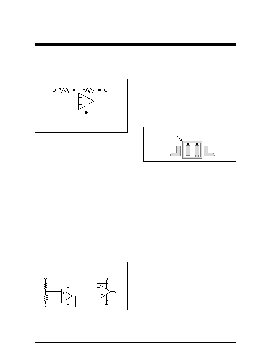
To use the internal mid-supply reference for an
inverting gain circuit, connect the VREF pin to the
non-inverting input, as shown in Figure 4-8. The
capacitor CB helps reduce power supply noise on the
output.
FIGURE 4-8:
Inverting gain circuit using
VREF (MCP6021 and MCP6023 only).
If you don’t need the mid-supply reference, leave the
VREF pin open.
4.7
Supply Bypass
With this family of operational amplifiers, the power
supply pin (VDD for single supply) should have a local
bypass capacitor (i.e., 0.01 F to 0.1 F) within 2 mm
for good, high-frequency performance. It also needs a
bulk capacitor (i.e., 1 F or larger) within 100 mm to
provide large, slow currents. This bulk capacitor can be
shared with nearby analog parts.
4.8
Unused Op Amps
An unused op amp in a quad package (MCP6024)
should be configured as shown in Figure 4-9. These
circuits prevent the output from toggling and causing
crosstalk. Circuit A can use any reference voltage
between the supplies, provides a buffered DC voltage,
and minimizes the supply current draw of the unused
op amp. Circuit B uses the minimum number of compo-
nents and operates as a comparator; it may draw more
current.
FIGURE 4-9:
Unused Op Amps.
4.9
PCB Surface Leakage
In applications where low input bias current is critical,
PCB (printed circuit board) surface-leakage effects
need to be considered. Surface leakage is caused by
humidity, dust or other contamination on the board.
Under low humidity conditions, a typical resistance
between nearby traces is 1012
Ω. A 5V difference would
cause 5 pA of current to flow, which is greater than the
MCP6021/1R/2/3/4 family’s bias current at +25°C
(1 pA, typ).
The easiest way to reduce surface leakage is to use a
guard ring around sensitive pins (or traces). The guard
ring is biased at the same voltage as the sensitive pin.
Figure 4-10 shows an example of this type of layout.
FIGURE 4-10:
Example Guard Ring
Layout.
1.
Non-inverting Gain and Unity-Gain Buffer.
a)
Connect the guard ring to the inverting input
pin (VIN–); this biases the guard ring to the
common mode input voltage.
b)
Connect the non-inverting pin (VIN+) to the
input with a wire that does not touch the
PCB surface.
2.
Inverting (Figure 4-10) and Transimpedance
Gain Amplifiers (convert current to voltage, such
as photo detectors).
a)
Connect the guard ring to the non-inverting
input pin (VIN+). This biases the guard ring
to the same reference voltage as the op
amp’s input (e.g., VDD/2 or ground).
b)
Connect the inverting pin (VIN–) to the input
with a wire that does not touch the PCB
surface.
4.10
High Speed PCB Layout
Due to their speed capabilities, a little extra care in the
PCB (Printed Circuit Board) layout can make a
significant difference in the performance of these op
amps. Good PC board layout techniques will help you
achieve the performance shown in Section 1.0 “Elec-
trical Characteristics” and Section 2.0 “Typical Per-
formance Curves”, while also helping you minimize
EMC (Electro-Magnetic Compatibility) issues.
Use a solid ground plane and connect the bypass local
capacitor(s) to this plane with minimal length traces.
This cuts down inductive and capacitive crosstalk.
VIN
RG
RF
VOUT
VREF
CB
VDD
MCP6144 (A)
MCP6144 (B)
R
VDD
Guard Ring
VIN–VIN+
相關(guān)PDF資料 |
PDF描述 |
|---|---|
| MCP604T-E/SL | QUAD OP-AMP, 4500 uV OFFSET-MAX, 2.8 MHz BAND WIDTH, PDSO14 |
| MCP604T-E/ST | QUAD OP-AMP, 4500 uV OFFSET-MAX, 2.8 MHz BAND WIDTH, PDSO14 |
| MCP607-I/PG | DUAL OP-AMP, 250 uV OFFSET-MAX, 0.155 MHz BAND WIDTH, PDIP8 |
| MCP607-I/SNG | DUAL OP-AMP, 250 uV OFFSET-MAX, 0.155 MHz BAND WIDTH, PDSO8 |
| MCP6142-E/MS | DUAL OP-AMP, 3000 uV OFFSET-MAX, 0.1 MHz BAND WIDTH, PDSO8 |
相關(guān)代理商/技術(shù)參數(shù) |
參數(shù)描述 |
|---|---|
| MCP6021R-E/MS | 制造商:MICROCHIP 制造商全稱:Microchip Technology 功能描述:Rail-to-Rail Input/Output, 10 MHz Op Amps |
| MCP6021R-E/OT | 制造商:MICROCHIP 制造商全稱:Microchip Technology 功能描述:Rail-to-Rail Input/Output, 10 MHz Op Amps |
| MCP6021R-E/P | 制造商:MICROCHIP 制造商全稱:Microchip Technology 功能描述:Rail-to-Rail Input/Output, 10 MHz Op Amps |
| MCP6021R-E/SL | 制造商:MICROCHIP 制造商全稱:Microchip Technology 功能描述:Rail-to-Rail Input/Output, 10 MHz Op Amps |
| MCP6021R-E/SN | 制造商:MICROCHIP 制造商全稱:Microchip Technology 功能描述:Rail-to-Rail Input/Output, 10 MHz Op Amps |
發(fā)布緊急采購,3分鐘左右您將得到回復(fù)。