- 您現(xiàn)在的位置:買賣IC網(wǎng) > PDF目錄296503 > MCP604T-E/SL QUAD OP-AMP, 4500 uV OFFSET-MAX, 2.8 MHz BAND WIDTH, PDSO14 PDF資料下載
參數(shù)資料
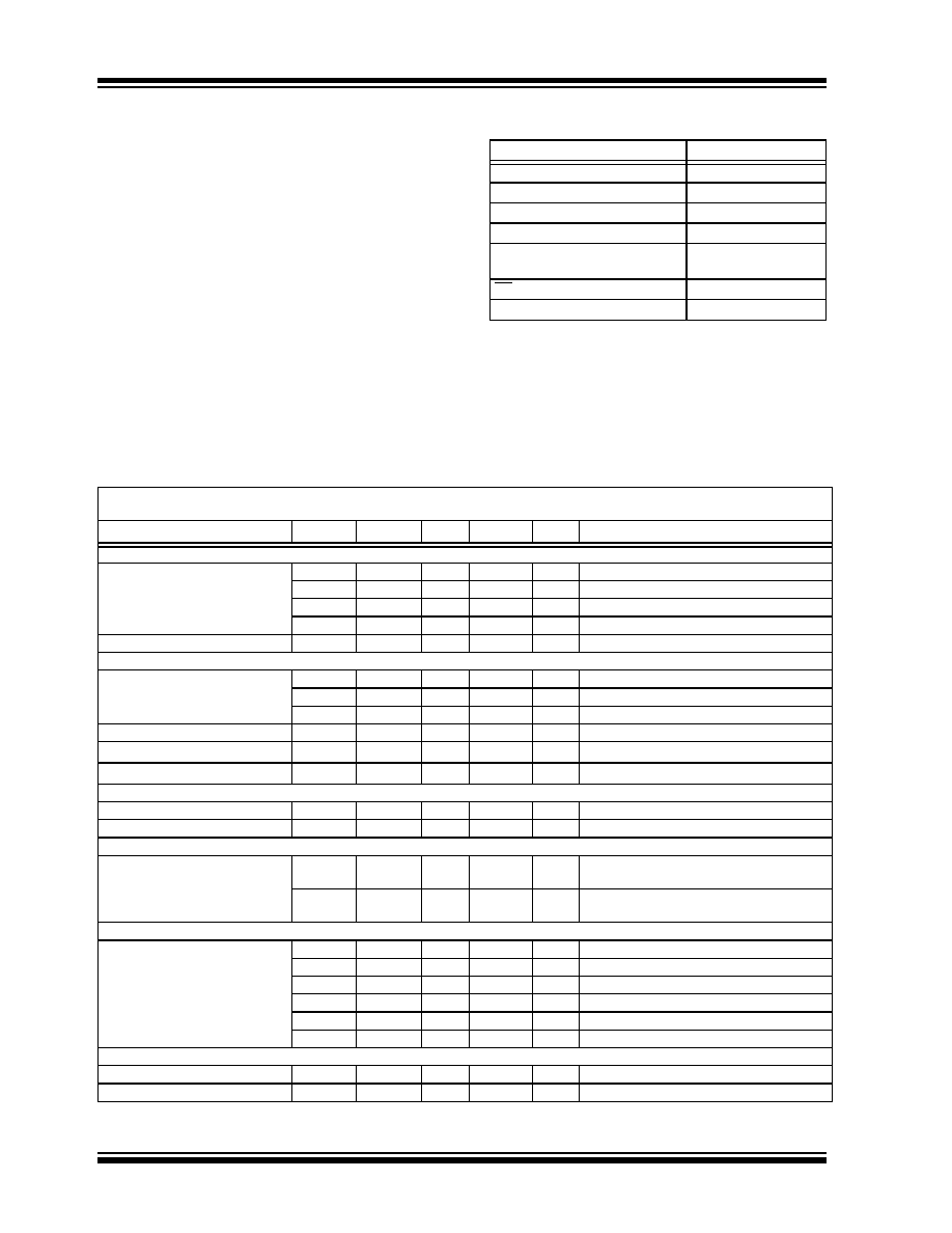
| 型號: | MCP604T-E/SL |
| 元件分類: | 運算放大器 |
| 英文描述: | QUAD OP-AMP, 4500 uV OFFSET-MAX, 2.8 MHz BAND WIDTH, PDSO14 |
| 封裝: | 0.150 INCH, PLASTIC, MS-012, SOIC-14 |
| 文件頁數(shù): | 12/28頁 |
| 文件大小: | 601K |
| 代理商: | MCP604T-E/SL |
第1頁第2頁第3頁第4頁第5頁第6頁第7頁第8頁第9頁第10頁第11頁當前第12頁第13頁第14頁第15頁第16頁第17頁第18頁第19頁第20頁第21頁第22頁第23頁第24頁第25頁第26頁第27頁第28頁
MCP601/2/3/4
DS21314F-page 2
2004 Microchip Technology Inc.
1.0
ELECTRICAL
CHARACTERISTICS
Absolute Maximum Ratings
VDD - VSS .........................................................................7.0V
All inputs and outputs...................... VSS - 0.3V to VDD + 0.3V
Difference Input voltage ........................................ |VDD - VSS|
Output Short Circuit Current...................................continuous
Current at Input Pin .......................................................±2 mA
Current at Output and Supply Pins .............................±30 mA
Storage temperature .....................................-65°C to +150°C
Junction temperature .................................................. +150°C
ESD protection on all pins (HBM; MM)
................ ≥ 3 kV; 200V
Notice: Stresses above those listed under “Maximum Rat-
ings” may cause permanent damage to the device. This is a
stress rating only and functional operation of the device at
those or any other conditions above those indicated in the
operational listings of this specification is not implied.
Exposure to maximum rating conditions for extended periods
may affect device reliability.
PIN FUNCTION TABLE
Name
Function
VIN+, VINA+, VINB+, VINC+, VIND+ Non-inverting Inputs
VIN–, VINA–, VINB–, VINC–, VIND– Inverting Inputs
VDD
Positive Power Supply
VSS
Negative Power Supply
VOUT, VOUTA, VOUTB, VOUTC,
VOUTD
Outputs
CS
Chip Select
NC
No Internal Connection
DC CHARACTERISTICS
Electrical Specifications: Unless otherwise specified, TA = +25°C, VDD = +2.7V to +5.5V, VSS = GND, VCM = VDD/2,
VOUT ≈ VDD/2 and RL = 100 k to VDD/2.
Parameters
Sym
Min
Typ
Max
Units
Conditions
Input Offset
Input Offset Voltage
VOS
-2
±0.7
+2
mV
Industrial Temperature
VOS
-3
±1
+3
mV
Extended Temperature
VOS
-4.5
±1
+4.5
mV
Input Offset Temperature Drift
VOS/TA
—±2.5
—
V/°C TA = -40°C to +125°C
Power Supply Rejection
PSRR
80
88
—
dB
VDD = 2.7V to 5.5V
Input Current and Impedance
Input Bias Current
IB
—1
—
pA
Industrial Temperature
IB
—20
60
pA
Extended Temperature
IB
—
450
5000
pA
Input Offset Current
IOS
—±1
—
pA
Common Mode Input Impedance
ZCM
—
1013||6
—
||pF
Differential Input Impedance
ZDIFF
—
1013||3
—
||pF
Common Mode
Common Mode Input Range
VCMR
VSS – 0.3
—
VDD – 1.2
V
Common Mode Rejection Ratio
CMRR
75
90
—
dB
VDD = 5.0V, VCM = -0.3V to 3.8V
Open-loop Gain
DC Open-loop Gain (large signal)
AOL
100
115
—
dB
RL = 25 k to VDD/2,
VOUT = 100 mV to VDD – 100 mV
AOL
95
110
—
dB
RL = 5 k to VDD/2,
VOUT = 100 mV to VDD – 100 mV
Output
Maximum Output Voltage Swing
VOL, VOH VSS + 15
—
VDD – 20
mV
RL = 25 k to VDD/2, Output overdrive = 0.5V
VOL, VOH VSS + 45
—
VDD – 60
mV
RL = 5 k to VDD/2, Output overdrive = 0.5V
Linear Output Voltage Swing
VOUT
VSS + 100
—
VDD – 100
mV
RL = 25 k to VDD/2, AOL ≥ 100 dB
VOUT
VSS + 100
—
VDD – 100
mV
RL = 5 k to VDD/2, AOL ≥ 95 dB
Output Short Circuit Current
ISC
—±22
—mA
VDD = 5.5V
ISC
—±12
—mA
VDD = 2.7V
Power Supply
Supply Voltage
VDD
2.7
—
5.5
V
Quiescent Current per Amplifier
IQ
—
230
325
A
IO = 0
Note 1:
These specifications are not tested in either the SOT-23 or TSSOP packages with date codes older than YYWW = 0408.
In these cases, the minimum and maximum values are by design and characterization only.
相關(guān)PDF資料 |
PDF描述 |
|---|---|
| MCP604T-E/ST | QUAD OP-AMP, 4500 uV OFFSET-MAX, 2.8 MHz BAND WIDTH, PDSO14 |
| MCP607-I/PG | DUAL OP-AMP, 250 uV OFFSET-MAX, 0.155 MHz BAND WIDTH, PDIP8 |
| MCP607-I/SNG | DUAL OP-AMP, 250 uV OFFSET-MAX, 0.155 MHz BAND WIDTH, PDSO8 |
| MCP6142-E/MS | DUAL OP-AMP, 3000 uV OFFSET-MAX, 0.1 MHz BAND WIDTH, PDSO8 |
| MCP631-E/SN | OP-AMP, 8000 uV OFFSET-MAX, 24 MHz BAND WIDTH, PDSO8 |
相關(guān)代理商/技術(shù)參數(shù) |
參數(shù)描述 |
|---|---|
| MCP604T-ESN | 制造商:MICROCHIP 制造商全稱:Microchip Technology 功能描述:2.7V to 6.0V Single Supply CMOS Op Amps |
| MCP604T-EST | 制造商:MICROCHIP 制造商全稱:Microchip Technology 功能描述:2.7V to 6.0V Single Supply CMOS Op Amps |
| MCP604T-I | 制造商:MICROCHIP 制造商全稱:Microchip Technology 功能描述:2.7V to 6.0V Single Supply CMOS Op Amps |
| MCP604T-I/SL | 功能描述:運算放大器 - 運放 Quad 2.7V RoHS:否 制造商:STMicroelectronics 通道數(shù)量:4 共模抑制比(最小值):63 dB 輸入補償電壓:1 mV 輸入偏流(最大值):10 pA 工作電源電壓:2.7 V to 5.5 V 安裝風格:SMD/SMT 封裝 / 箱體:QFN-16 轉(zhuǎn)換速度:0.89 V/us 關(guān)閉:No 輸出電流:55 mA 最大工作溫度:+ 125 C 封裝:Reel |
| MCP604T-I/ST | 功能描述:運算放大器 - 運放 Quad 2.7V RoHS:否 制造商:STMicroelectronics 通道數(shù)量:4 共模抑制比(最小值):63 dB 輸入補償電壓:1 mV 輸入偏流(最大值):10 pA 工作電源電壓:2.7 V to 5.5 V 安裝風格:SMD/SMT 封裝 / 箱體:QFN-16 轉(zhuǎn)換速度:0.89 V/us 關(guān)閉:No 輸出電流:55 mA 最大工作溫度:+ 125 C 封裝:Reel |
發(fā)布緊急采購,3分鐘左右您將得到回復。