- 您現(xiàn)在的位置:買賣IC網(wǎng) > PDF目錄67987 > MCP7940NT-I/ST REAL TIME CLOCK, PDSO8 PDF資料下載
參數(shù)資料
| 型號: | MCP7940NT-I/ST |
| 元件分類: | 時鐘/數(shù)據(jù)恢復(fù)及定時提取 |
| 英文描述: | REAL TIME CLOCK, PDSO8 |
| 封裝: | 4.40 MM, PLASTIC, TSSOP-8 |
| 文件頁數(shù): | 7/36頁 |
| 文件大?。?/td> | 551K |
| 代理商: | MCP7940NT-I/ST |
第1頁第2頁第3頁第4頁第5頁第6頁當(dāng)前第7頁第8頁第9頁第10頁第11頁第12頁第13頁第14頁第15頁第16頁第17頁第18頁第19頁第20頁第21頁第22頁第23頁第24頁第25頁第26頁第27頁第28頁第29頁第30頁第31頁第32頁第33頁第34頁第35頁第36頁
2011 Microchip Technology Inc.
DS25010A-page 15
MCP7940N
5.2
RTCC/SRAM
5.2.1
SRAM BYTE WRITE
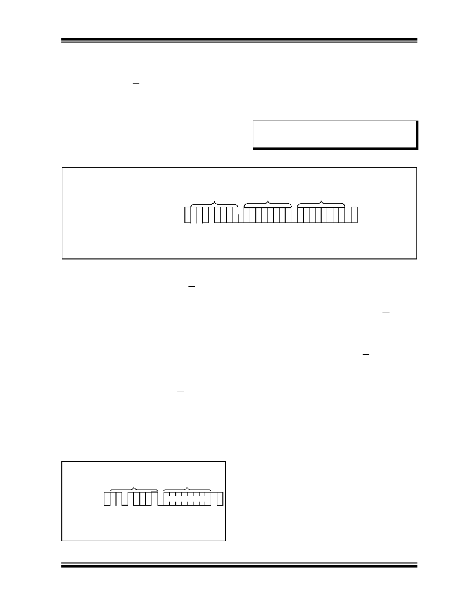
Following the Start condition from the master, the
control code and the R/W bit (which is a logic low) are
clocked onto the bus by the master transmitter. This
indicates to the addressed slave receiver that a byte
with a word address will follow after it has generated an
Acknowledge
bit
during
the
ninth
clock
cycle.
Therefore, the next byte transmitted by the master is
the word address and will be written into the Address
Pointer of the MCP7940N. After receiving another
Acknowledge signal from the MCP7940N, the master
device transmits the data word to be written into the
addressed
memory
location.
The
MCP7940N
acknowledges again and the master generates a Stop
condition. After a Byte Write command, the internal
address counter will point to the address location
following the one that was just written.
FIGURE 5-3:
SRAM BYTE WRITE
5.2.2
READ OPERATION
Read operations are initiated in the same way as write
operations with the exception that the R/W bit of the
control byte is set to one. There are three basic types
of read operations: current address read, random read,
and sequential read.
5.2.2.1
Current Address Read
The MCP7940N contains an address counter that
maintains the address of the last word accessed,
internally incremented by one. Therefore, if the
previous read access was to address n (n is any legal
address), the next current address read operation
would access data from address n + 1.
Upon receipt of the control byte with R/W bit set to one,
the MCP7940N issues an Acknowledge and transmits
the 8-bit data word. The master will not acknowledge
the transfer but does generate a Stop condition and the
MCP7940N discontinues transmission (Figure 5-4).
FIGURE 5-4:
CURRENT ADDRESS
READ
5.2.2.2
Random Read
Random read operations allow the master to access
any memory location in a random manner. To perform
this type of read operation, first the word address must
be set. This is done by sending the word address to the
MCP7940N as part of a write operation (R/W bit set to
‘0’). After the word address is sent, the master
generates a Start condition following the Acknowledge.
This terminates the write operation, but not before the
internal Address Pointer is set. Then, the master issues
the control byte again but with the R/W bit set to a one.
The MCP7940N will then issue an Acknowledge and
transmit the 8-bit data word. The master will not
acknowledge the transfer but it does generate a Stop
condition which causes the MCP7940N to discontinue
transmission (Figure 5-5). After a Random Read
command, the internal address counter will point to the
address location following the one that was just read.
Note:
Addressing undefined SRAM locations will
result
in
the
MCP7940N
not
acknowledging the address.
BUS ACTIVITY
MASTER
SDA LINE
BUS ACTIVITY
S
T
A
R
T
CONTROL
BYTE
ADDRESS
BYTE
DATA
S
T
O
P
A
C
K
A
C
K
A
C
K
S 110 1
0
1 11
P
x
x = don’t care for 1K devices
BUS ACTIVITY
MASTER
SDA LINE
BUS ACTIVITY
P
S
T
O
P
CONTROL
BYTE
S
T
A
R
T
DATA
A
C
K
N
O
A
C
K
10
11
1
BYTE
11 1
相關(guān)PDF資料 |
PDF描述 |
|---|---|
| MCP7940NT-I/SN | REAL TIME CLOCK, PDSO8 |
| MCP7940NT-I/MS | REAL TIME CLOCK, PDSO8 |
| MCP79411-I/SN | REAL TIME CLOCK, PDSO8 |
| MCP79411-I/MNY | REAL TIME CLOCK, PDSO8 |
| MCP79410-I/ST | REAL TIME CLOCK, PDSO8 |
相關(guān)代理商/技術(shù)參數(shù) |
參數(shù)描述 |
|---|---|
| MCP79410 | 制造商:MICROCHIP 制造商全稱:Microchip Technology 功能描述:I2C? Real-Time Clock/Calendar with EEPROM, SRAM, Unique ID and Battery Switchover |
| MCP79410_13 | 制造商:MICROCHIP 制造商全稱:Microchip Technology 功能描述:Battery-Backed I2Ca?¢ Real-Time Clock/Calendar with EEPROM and Unique ID |
| MCP79410-I/MNY | 制造商:Microchip Technology Inc 功能描述:I2C GP RTCC, 1KB EE, 64B SRAM, ID - Rail/Tube |
| MCP79410-I/MS | 功能描述:實時時鐘 I2C GP RTCC 1Kb EE 64B SRAM ID RoHS:否 制造商:Microchip Technology 功能:Clock, Calendar. Alarm RTC 總線接口:I2C 日期格式:DW:DM:M:Y 時間格式:HH:MM:SS RTC 存儲容量:64 B 電源電壓-最大:5.5 V 電源電壓-最小:1.8 V 最大工作溫度:+ 85 C 最小工作溫度: 安裝風(fēng)格:Through Hole 封裝 / 箱體:PDIP-8 封裝:Tube |
| MCP79410-I/P | 制造商:Microchip Technology Inc 功能描述:I2C GP RTCC, 1KB EE, 64B SRAM, ID - Rail/Tube 制造商:Microchip Technology Inc 功能描述:RTCC 12C 1K EE 64B SRAM 8PDIP |
發(fā)布緊急采購,3分鐘左右您將得到回復(fù)。