- 您現(xiàn)在的位置:買(mǎi)賣(mài)IC網(wǎng) > PDF目錄1953 > MCW1001AT-I/SS (Microchip Technology)IC INTERFACE SOCKET XLP 28-SSOP PDF資料下載
參數(shù)資料
| 型號(hào): | MCW1001AT-I/SS |
| 廠(chǎng)商: | Microchip Technology |
| 文件頁(yè)數(shù): | 7/66頁(yè) |
| 文件大小: | 0K |
| 描述: | IC INTERFACE SOCKET XLP 28-SSOP |
| 標(biāo)準(zhǔn)包裝: | 2,100 |
| 系列: | * |
第1頁(yè)第2頁(yè)第3頁(yè)第4頁(yè)第5頁(yè)第6頁(yè)當(dāng)前第7頁(yè)第8頁(yè)第9頁(yè)第10頁(yè)第11頁(yè)第12頁(yè)第13頁(yè)第14頁(yè)第15頁(yè)第16頁(yè)第17頁(yè)第18頁(yè)第19頁(yè)第20頁(yè)第21頁(yè)第22頁(yè)第23頁(yè)第24頁(yè)第25頁(yè)第26頁(yè)第27頁(yè)第28頁(yè)第29頁(yè)第30頁(yè)第31頁(yè)第32頁(yè)第33頁(yè)第34頁(yè)第35頁(yè)第36頁(yè)第37頁(yè)第38頁(yè)第39頁(yè)第40頁(yè)第41頁(yè)第42頁(yè)第43頁(yè)第44頁(yè)第45頁(yè)第46頁(yè)第47頁(yè)第48頁(yè)第49頁(yè)第50頁(yè)第51頁(yè)第52頁(yè)第53頁(yè)第54頁(yè)第55頁(yè)第56頁(yè)第57頁(yè)第58頁(yè)第59頁(yè)第60頁(yè)第61頁(yè)第62頁(yè)第63頁(yè)第64頁(yè)第65頁(yè)第66頁(yè)

2011 Microchip Technology Inc.
Preliminary
DS70671A-page 15
MCW1001A
2.0
EXTERNAL CONNECTIONS
2.1
Oscillator
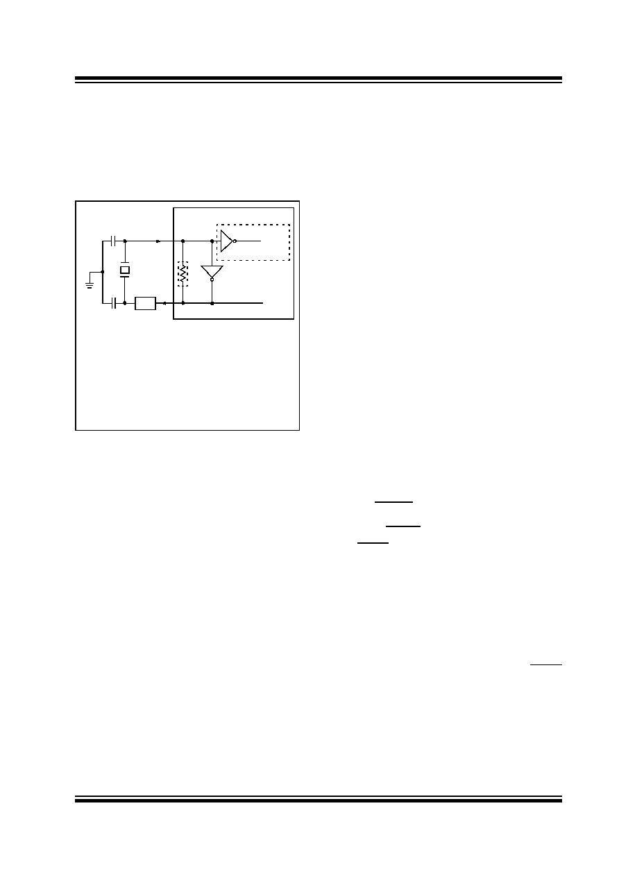
MCW1001A devices are designed to operate from a
fixed 8 MHz crystal clock input, as shown in Figure 2-1.
FIGURE 2-1:
CRYSTAL OSCILLATOR
OPERATION
2.2
VDD AND VSS PINS
2.2.1
DECOUPLING CAPACITORS
The use of decoupling capacitors on all power supply
pins, such as VDD, VSS, are required.
Consider the following criteria when using decoupling
capacitors:
Value and type of capacitor: A 0.1 μF (100 nF)
and 10–20V capacitor is recommended. The
capacitor should be a low-ESR device with a
resonance frequency in the range of 200 MHz and
higher. Ceramic capacitors are also
recommended.
Placement on the printed circuit board: The
decoupling capacitors should be placed as close
to the pins as possible. It is recommended to
place the capacitors on the same side of the
board as the device. If space is constricted, the
capacitor can be placed on another layer of the
PCB using a via; however, ensure that the trace
length from the pin to the capacitor is not greater
than 0.25 inch (6 mm).
Handling high frequency noise: If the board is
experiencing high frequency noise (upward of
tens of MHz), add a second ceramic type capaci-
tor in parallel to the above described decoupling
capacitor. The value of the second capacitor can
be in the range of 0.01 μF to 0.001 μF. Place this
second capacitor next to each primary decoupling
capacitor. In high-speed circuit designs, consider
implementing a decade pair of capacitances as
close to the power and ground pins as possible
(e.g., 0.1 μF in parallel with 0.001 μF).
Maximizing performance: On the board layout
from the power supply circuit, run the power and
return traces to the device pins. This ensures that
the decoupling capacitors are first in the power
chain. It is equally important to keep the trace
length between the capacitor and the power pins
to a minimum, thereby reducing PCB trace induc-
tance.
2.2.2
TANK CAPACITORS
On PCB boards with power traces running longer than
six inches in length, it is suggested to use a tank capac-
itor for integrated circuits, including microcontrollers, to
supply a local power source. The value of the tank
capacitor should be determined based on the trace
resistance that connects the power supply source to
the device, and the maximum current drawn by the
device in the application. In other words, select the tank
capacitor so that it meets the acceptable voltage sag at
the device. Typical values range from 4.7 μF to 47 μF.
2.2.3
VOLTAGE REGULATOR PINS
(VCAP)
A low-ESR (<5) capacitor is required on the VCAP pin
to stabilize the voltage regulator output voltage. The
VCAP pin must not be connected to VDD and must use
a capacitor of 10 μF connected to ground. The type can
be ceramic or tantalum. For example, Murata
GRM21BF50J106ZE01 (10 μF, 6.3V) or equivalent.
2.3
RESET/PoR
2.3.1
RESET PIN
The RESET pin provides a method for triggering an
external Reset of the device. Holding the pin low gen-
erates a Reset. These devices have a noise filter in the
Reset path that detects and ignores small pulses.
2.3.2
PoR
A power-on Reset (PoR) pulse is generated on-chip
whenever VDD rises above a certain threshold. This
allows the device to start in the initialized state when
VDD is adequate for operation.
To take advantage of the PoR circuitry, tie the RESET
pin through a resistor (1 k to 10 k) to VDD. This will
eliminate external RC components usually needed to
create a PoR delay.
When the device starts normal operation (i.e., exits the
Reset
condition),
device
operating
parameters
(voltage, frequency, temperature, etc.) must be met to
ensure the operation. If these conditions are not
achieved, the device must be held in Reset until the
operating conditions are met.
C1(3)
C2(3)
8 MHz
OSC2
RS(1)
OSC1
RF(2)
To Internal Logic
Note 1:
A series resistor, RS, may be required for
crystals with a low drive strength specification
or when using large loading capacitors.
2:
The feedback resistor, RF , is typically 1.5 M
Ω
(approx).
3:
The load capacitors’ value should be derived
from the capacitive loading specification
provided by the crystal manufacture.
MCW1001A
相關(guān)PDF資料 |
PDF描述 |
|---|---|
| MCZ145010EG | IC SMOKE DETECT PHOTOELEC 16SOIC |
| MCZ145012EG | IC SMOKE DETECT PHOTOELEC 16SOIC |
| MCZ33094EG | IC IGNITION CONTROL 12V 16-SOIC |
| MCZ33287EG | IC DRIVER DUAL LOSIDE MON 20SOIC |
| MCZ33290EF | IC SER LNK INTER ISO KLINE 8SOIC |
相關(guān)代理商/技術(shù)參數(shù) |
參數(shù)描述 |
|---|---|
| MCW1011 | 制造商:MINMAX 制造商全稱(chēng):Minmax Technology Co., Ltd. 功能描述:2W, Wide Input Range SIP, Single Output DC/DC Converters |
| MCW1012 | 制造商:MINMAX 制造商全稱(chēng):Minmax Technology Co., Ltd. 功能描述:2W, Wide Input Range SIP, Single Output DC/DC Converters |
| MCW1013 | 制造商:MINMAX 制造商全稱(chēng):Minmax Technology Co., Ltd. 功能描述:2W, Wide Input Range SIP, Single Output DC/DC Converters |
| MCW1021 | 制造商:MINMAX 制造商全稱(chēng):Minmax Technology Co., Ltd. 功能描述:2W, Wide Input Range SIP, Single Output DC/DC Converters |
| MCW1022 | 制造商:MINMAX 制造商全稱(chēng):Minmax Technology Co., Ltd. 功能描述:2W, Wide Input Range SIP, Single Output DC/DC Converters |
發(fā)布緊急采購(gòu),3分鐘左右您將得到回復(fù)。