- 您現(xiàn)在的位置:買賣IC網(wǎng) > PDF目錄371109 > MHPM6B15N120SS (MOTOROLA INC) Hybrid Power Module PDF資料下載
參數(shù)資料
| 型號: | MHPM6B15N120SS |
| 廠商: | MOTOROLA INC |
| 元件分類: | IGBT 晶體管 |
| 英文描述: | Hybrid Power Module |
| 中文描述: | 10 A, 1200 V, N-CHANNEL IGBT |
| 文件頁數(shù): | 7/10頁 |
| 文件大小: | 265K |
| 代理商: | MHPM6B15N120SS |

7
Motorola IGBT Device Data
APPLICATION INFORMATION
These modules are designed to be used as the power
stage of a three–phase AC induction motor drive. They may
be used for up to 460 VAC applications. Switching frequen-
cies up to 15 kHz were considered in the design.
Gate resistance recommendations have been listed.
These choices were based on the common gate drive circuit
shown in Figure 16. However, significant improvements in
Eoff may be gained by either of two methods: use of a nega-
tive gate bias, or use of the gate drive shown in Figure 17.
Separate turn–on and turn–off gate resistors give the best re-
sults; in this case, RG(off) should be chosen as small as pos-
sible while limiting current to prevent damage to the gate
drive IC. Designers should also note that turn–on and turn–
off delay times are measured from the rising and falling
edges of the gate drive output, not the gate voltage wave-
form.
Since all three modules use similar technology, most of the
graphs showing typical performance have been normalized.
Actual values are listed for each size in the table, “Electrical
Characteristics.” Data on the graphs reflect performance us-
ing the common gate drive circuit shown in Figure 16.
The first three curves, showing DC characteristics, are
normalized for ICmax. The devices all perform similarly at
rated current. The curves extend to IC(pk), the maximum al-
lowable instantaneous current.
The next two graphs, turn–off and turn–on times versus IC,
are also normalized for ICmax. In addition, the time scales are
normalized. Turn–off times are normalized to td(off) at 25
°
C at
rated current with recommended RG, while turn–on times are
normalized to tr at 25
°
C at rated current with recommended
RG.
The graphs showing switching times as a function of RG
are similarly normalized. RG has been normalized to the rec-
ommended value listed under “Electrical Characteristics.”
The time axes are normalized exactly as for the correspond-
ing graphs showing variation with IC.
Similar transformations have been made for the next two
figures, showing Eon and Eoff. Energies have been normal-
ized to Eoff at 25
°
C at ICmax with the recommended RG. IC
has been normalized to ICmax, and RG has been normalized
to the recommended value.
Reverse recovery characteristics are also normalized. IC
has again been normalized to ICmax. Reverse recovery time
trr has been normalized to trr at 25
°
C at ICmax. Peak reverse
recovery current Irrm has been normalized to Irrm at 25
°
C at
ICmax, then multiplied by 10.
Capacitance has been normalized to device rated ICmax.
Since all modules are rated for the same voltage, the voltage
scale on Figure 11 does not need to be normalized.
Typical transient thermal impedance is shown for a diode
and for an IGBT. All diodes behave quite similarly, as do all
IGBTs.
The last two graphs, VGE versus QG and RBSOA, are not
normalized.
Many issues beyond the ratings must be considered in a
system design. Dynamic characteristics can all be affected
by external circuit parameters. For example, excessive bus
inductance can dramatically increase voltage overshoot dur-
ing switching, increasing the switching energy. The choice of
gate drive IC can have quite a large effect on rise and fall
times, corresponding to differences in switching energies. In
many cases, this can be compensated by simply changing
the gate resistor accordingly — a gate driver with a lower
drive capability requires a smaller gate resistor. Ultimately,
the module must be tested in the final system to characterize
its performance.
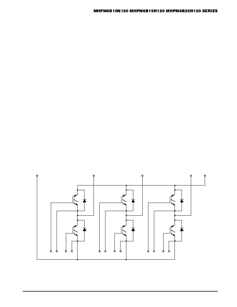
Figure 18. Schematic of Module, Showing Pin–Out
4
D5
D6
7
Q5
Q6
6
9
8
5
3
D3
D4
11
Q3
Q4
10
13
12
2
D1
D2
15
Q1
Q2
14
17
16
1
相關(guān)PDF資料 |
PDF描述 |
|---|---|
| MHPM6B25N120SL | Hybrid Power Module |
| MHPM6B5A120D | SWITCH, 20A, CO WITHOUT OFF; Poles, No. of:1; Current rating:20A; Power, switching AC3 max:6.5kW RoHS Compliant: Yes |
| MHPM6B10A120D | Hybrid Power Module |
| MHPM6B15A120D | Hybrid Power Module |
| MHPM7A15S120DC3 | MAINS SWITCH, T0-2-1/E; Poles, No. of:3; Current rating:20A; Length / Height, external:48mm; Width, external:48mm RoHS Compliant: NA |
相關(guān)代理商/技術(shù)參數(shù) |
參數(shù)描述 |
|---|---|
| MHPM6B20E60D3 | 制造商:MOTOROLA 制造商全稱:Motorola, Inc 功能描述:Hybrid Power Module |
| MHPM6B25N120SL | 制造商:MOTOROLA 制造商全稱:Motorola, Inc 功能描述:Hybrid Power Module |
| MHPM6B25N120SS | 制造商:MOTOROLA 制造商全稱:Motorola, Inc 功能描述:Hybrid Power Module |
| MHPM6B2A60D | 制造商:MOTOROLA 制造商全稱:Motorola, Inc 功能描述:Hybrid Power Module |
| MHPM6B5A120D | 制造商:MOTOROLA 制造商全稱:Motorola, Inc 功能描述:Hybrid Power Module |
發(fā)布緊急采購,3分鐘左右您將得到回復(fù)。