- 您現(xiàn)在的位置:買賣IC網(wǎng) > PDF目錄379320 > MHW927B (MOTOROLA INC) 6.0 W 824 to 849 MHz RF LINEAR POWER AMPLIFIERS PDF資料下載
參數(shù)資料
| 型號: | MHW927B |
| 廠商: | MOTOROLA INC |
| 元件分類: | 衰減器 |
| 英文描述: | 6.0 W 824 to 849 MHz RF LINEAR POWER AMPLIFIERS |
| 中文描述: | 824 MHz - 849 MHz RF/MICROWAVE NARROW BAND HIGH POWER AMPLIFIER |
| 文件頁數(shù): | 1/6頁 |
| 文件大?。?/td> | 166K |
| 代理商: | MHW927B |
1
MHW927A MHW927B
MOTOROLA RF DEVICE DATA
Motorola, Inc. 1994
The RF Line
Designed specifically for the United States digital 3.0 W, mobile radio. The
MHW927A/B are capable of wide power range control, operate from a 12.5 V
supply and require 1.0 mW of RF input power.
MHW927A Operates from a 9.5 Volt Bias Supply (VB)
MHW927B Operates from a 8.0 Volt Bias Supply (VB)
Specified 12.5 Volt Characteristics for MHW927A/B:
RF Input Power — 1.0 mW (0 dBm) Max
RF Output Power — 6.0 W
Power Gain — 40 dB Typ
Harmonics — –30 dBc Max @ 2 f0
Linearity (IMD) — –29 dBc Max for 3rd Order; –34 dBc Max for 5th Order
New Biasing and Control Techniques Providing Dynamic Range and Control Circuit
Bandwidth Ideal for USDC
50
Input/Output Impedances
Guaranteed Stability and Ruggedness
MAXIMUM RATINGS
(Recommended Values for Safe Operation — Not Guaranteed Performance)
Rating
Symbol
Value
Unit
DC Supply Voltage
VS2, VS3
VB
Pin
Pout
TC
Tstg
16.5
Vdc
DC Bias Voltage
10
Vdc
RF Input Power
MHW927A, B
3.0
mW
RF Output Power
13
W
Operating Case Temperature Range
–30 to +100
°
C
°
C
Storage Temperature Range
–30 to +100
ELECTRICAL CHARACTERISTICS
(VS2 = VS3 = 12.5 Vdc; VB = 9.5 Vdc (MHW927A); VB = 8.0 Vdc (MHW927B); Pin
≤
1.0 mW
(MHW927A/B); TC = +25
°
C, 50 ohm system, unless otherwise noted)
Characteristic
Symbol
Min
Typ
Max
Unit
Frequency Range
BW
824
—
849
MHz
Input Power (Pout = 6.0 W) (1)
Efficiency (Pout = 6.0 W) (1)
Efficiency, Two Tone (Pout (Avg.) = 6.0 W; f1 & f2 10 kHz apart) (1)
Input VSWR (Pout = 6.0 W) (1)
Harmonics (Pout = 6.0 W) (1)
Pin
η
1
η
2
—
—
1.0
mW
28
30
—
%
28
30
—
%
VSWRin
—
—
—
2.5:1
—
2 f0
3 f0
—
—
—
—
–30
–45
dBc
Noise Power (In 30 kHz Bandwidth, 45 MHz Above f0; TC = +25
°
C to TC = +100
°
C;
Pout = 6.0 W) (1)
Linearity (Pout (Avg.) = 6.0 W; f1 & f2 are 10 kHz apart) (1) 3rd Order IMD
—
—
—
–82
dBm
5th Order IMD
—
—
—
–31
–36
–29
–34
dBc
Load Mismatch Stress (VS2 = VS3 = 16 Vdc; Pout = 12.5 W; Pulsed at 50% Duty
Cycle; Load VSWR = 20:1, All Phase Angles At Frequency of Test) (1)
ψ
No Degradation
In Output Power Between
Before and After Test
Stability (VS2 = VS3 = 10 to 16 Vdc; Pout = 0.012 to 12 W;
Load VSWR = 4:1, All Phase Angles At Frequency of Test) (1)
—
All Spurious Outputs
More Than 70 dB
Below Desired Signal
NOTE:
1. Adjust Pin for Specified Pout.
Preferred
devices are Motorola recommended choices for future use and best overall value.
Order this document
by MHW927A/D
SEMICONDUCTOR TECHNICAL DATA
6.0 W
824 to 849 MHz
RF LINEAR
POWER AMPLIFIERS
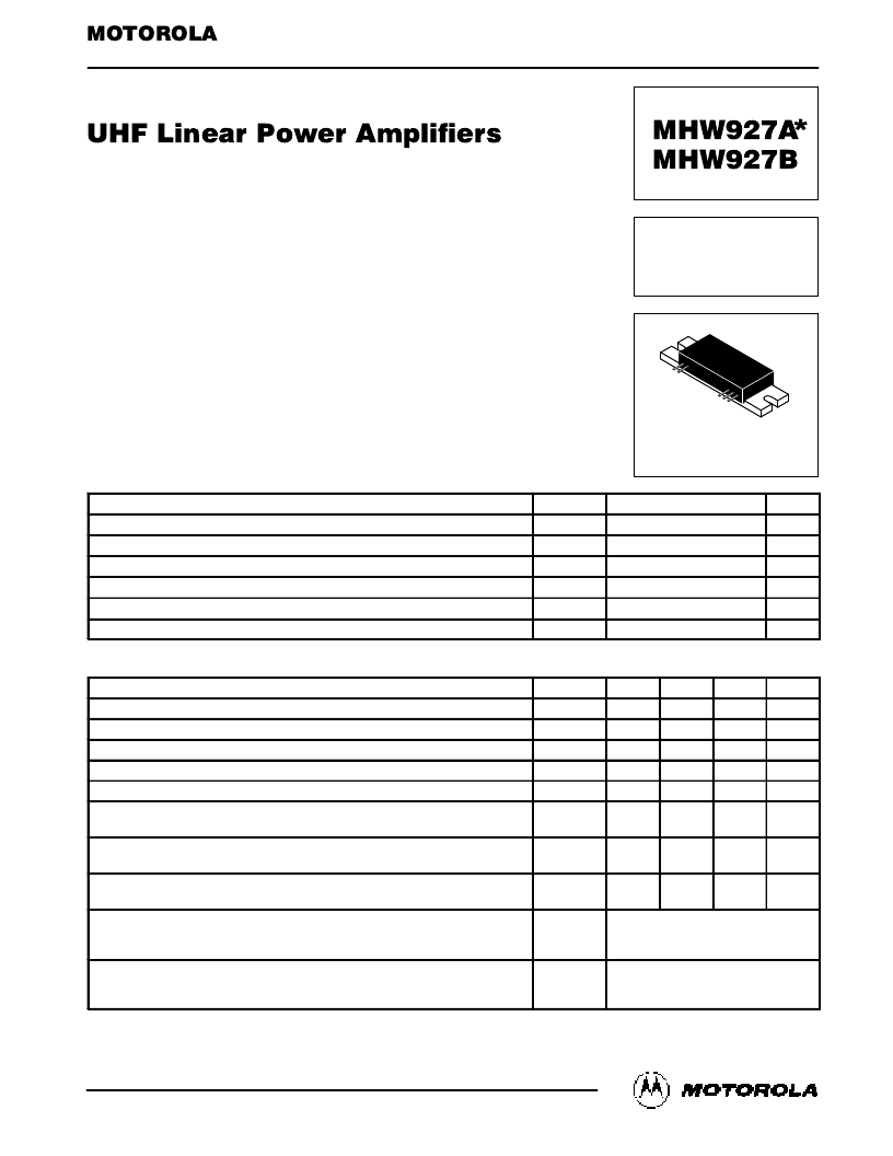
CASE 301AA–01, STYLE 1
*Motorola Preferred Device
REV 6
相關(guān)PDF資料 |
PDF描述 |
|---|---|
| MJ10042 | NPN SILICON POWER DARLINGTON TRANSISTOR |
| MJ10045 | NPN SILICON POWER DARLINGTON TRANSISTOR |
| MJ10048 | NPN SILICON POWER DARLINGTON TRANSISTOR |
| MJ13070 | NPN SILICON POWER TRANSISTORS |
| MJ13071 | NPN SILICON POWER TRANSISTORS |
相關(guān)代理商/技術(shù)參數(shù) |
參數(shù)描述 |
|---|---|
| MHW930 | 制造商:MOTOROLA 制造商全稱:Motorola, Inc 功能描述:30 W 925.960 MHz RF POWER AMPLIFIER |
| MHW932 | 制造商:MOTOROLA 制造商全稱:Motorola, Inc 功能描述:32 W 890 to 915 MHz RF POWER AMPLIFIER |
| MHW953 | 制造商:MOTOROLA 制造商全稱:Motorola, Inc 功能描述:3.5 W 890 to 915 MHz RF POWER AMPLIFIERS |
| MHW954 | 制造商:MOTOROLA 制造商全稱:Motorola, Inc 功能描述:3.5 W 890 to 915 MHz RF POWER AMPLIFIERS |
| MHWJ7182CN | 制造商:Rochester Electronics LLC 功能描述: 制造商:Freescale Semiconductor 功能描述: |
發(fā)布緊急采購,3分鐘左右您將得到回復(fù)。