- 您現(xiàn)在的位置:買賣IC網(wǎng) > PDF目錄383612 > MIC4830YMM (MICREL INC) Low Noise 180Vp-p EL Driver PDF資料下載
參數(shù)資料
| 型號: | MIC4830YMM |
| 廠商: | MICREL INC |
| 元件分類: | 顯示驅(qū)動器 |
| 英文描述: | Low Noise 180Vp-p EL Driver |
| 中文描述: | EL DISPLAY DRIVER, PDSO8 |
| 封裝: | ROHS COMPLIANT, MSOP-8 |
| 文件頁數(shù): | 3/12頁 |
| 文件大小: | 846K |
| 代理商: | MIC4830YMM |
Micrel
MIC4830
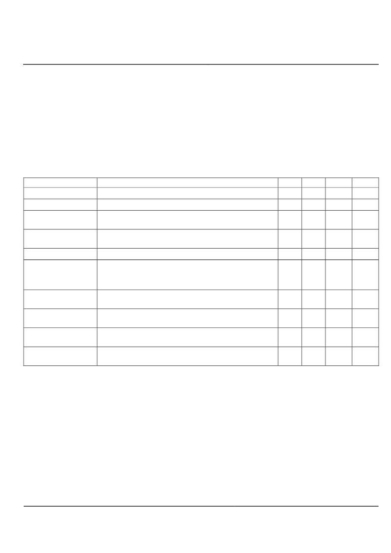
Absolute Maximum Ratings
(1)
September 2007
3
M9999-091307
(408) 955-1690
Supply Voltage (V
DD
)...................................... –0.5V to 6.0V
Output Voltage (V
CS
)..................................... –0.5V to 120V
EL Lamp Terminals (VA, VB)................................. V
CS
+ 3V
Switch Voltage (Vsw)…………………………..-0.5V to 120V
Frequency Control Voltage
(V
RSW
,
V
REL
)...................................–0.5V to (V
DD
+0.3V)
Storage Temperature (T
S
).........................–65°C to +150°C
ESD Rating
(4)
...............................................................1.5kV
Operating Ratings
(2)
Supply Voltage (V
DD
)....................................+1.8V to +5.5V
Lamp Drive Frequency (f
EL
) ....................... 60Hz to 1000Hz
Switching Frequency (f
SW
).........................65kHz to 250kHz
Ambient Temperature (T
A
)..........................–40°C to +85°C
Package Thermal Resistance
MSOP (
θ
JA
)......................................................206°C/W
MLF
-8L (
θ
JA
).....................................................63°C/W
Electrical Characteristics
(5)
V
IN
= V
DD
= 3.0V, R
SW
= 332K
, R
EL
= 1.78M
. T
A
= 25°C unless otherwise specified.
Bold
values indicate
–
40°C
≤
T
A
≤
+85°C.
Parameter
Condition
Min
Typ
Max
Units
On-resistance
I
SW
= 100mA
3.8
7
Ohm
CS Voltage Variation
V
DD
= 1.8V to 5.5V
76
88
99
V
Enable Input Low
Voltage (turn-off)
V
DD
= 1.8V to 5.5V
0.5
V
Enable Input High
Voltage (turn-on)
V
DD
= 1.8V to 5.5V
V
DD
-
0.5
V
Shutdown current
R
SW
Resistor = LOW; R
EL
Resistor = LOW; V
DD
= 5.5V
0.01
0.5
μ
A
Input supply current
R
SW
Resistor
= HIGH;
R
EL
Resistor
= HIGH;
V
CS
= 90V; V
A
, V
B
OPEN
45
75
μ
A
Input current including
inductor
V
IN
= V
DD
= 3.2V; Rsw = 290K
; Rel = 1.78M
;
L=220μH; Rout=10k
; Lamp = 2in
2
15
mA
V
A
–V
B
output drive
frequency
R
EL
=1.78M
158
200
242
Hz
Switching transistor
frequency
R
SW
=332K
90
112
134
kHz
Switching transistor
duty cycle
90
%
Notes:
1. Exceeding the absolute maximum rating may damage the device.
2.
The device is not guaranteed to function outside its operating rating.
3.
The maximum allowable power dissipation of any T
(ambient temperature) is P
D(max)
= (T
J(max)
– T
A
) /
θ
JA
. Exceeding the maximum allowable
power dissipation will result in excessive die temperature.
4.
Devices are ESD sensitive. Handling precautions recommended. Human body model, 1.5k in series with 100pF.
5.
Specification for packaged product only.
相關(guān)PDF資料 |
PDF描述 |
|---|---|
| MIC4832 | Low Noise 220Vp-p EL Driver |
| MIC4832YML | Low Noise 220Vp-p EL Driver |
| MIC4832YMM | Low Noise 220Vp-p EL Driver |
| MIC49150 | 1.5A Low Voltage LDO Regulator w/Dual Input Voltages |
| MIC49150-0.9BMM | 1.5A Low Voltage LDO Regulator w/Dual Input Voltages |
相關(guān)代理商/技術(shù)參數(shù) |
參數(shù)描述 |
|---|---|
| MIC4830YMM TR | 功能描述:LED照明驅(qū)動器 180Vpp Low Noise EL Driver RoHS:否 制造商:STMicroelectronics 輸入電壓:11.5 V to 23 V 工作頻率: 最大電源電流:1.7 mA 輸出電流: 最大工作溫度: 安裝風(fēng)格:SMD/SMT 封裝 / 箱體:SO-16N |
| MIC4832 | 制造商:MICREL 制造商全稱:Micrel Semiconductor 功能描述:Low Noise 220VPP EL Driver |
| MIC4832_09 | 制造商:MICREL 制造商全稱:Micrel Semiconductor 功能描述:Low Noise 220VPP EL Driver |
| MIC4832YML | 制造商:MICREL 制造商全稱:Micrel Semiconductor 功能描述:Low Noise 220Vp-p EL Driver |
| MIC4832YML TR | 功能描述:LED照明驅(qū)動器 220Vpp Low Noise EL Driver RoHS:否 制造商:STMicroelectronics 輸入電壓:11.5 V to 23 V 工作頻率: 最大電源電流:1.7 mA 輸出電流: 最大工作溫度: 安裝風(fēng)格:SMD/SMT 封裝 / 箱體:SO-16N |
發(fā)布緊急采購,3分鐘左右您將得到回復(fù)。