- 您現(xiàn)在的位置:買賣IC網(wǎng) > PDF目錄26831 > MK74CB214R CB SERIES, LOW SKEW CLOCK DRIVER, 7 TRUE OUTPUT(S), 0 INVERTED OUTPUT(S), PDSO20 PDF資料下載
參數(shù)資料
| 型號(hào): | MK74CB214R |
| 元件分類: | 時(shí)鐘及定時(shí) |
| 英文描述: | CB SERIES, LOW SKEW CLOCK DRIVER, 7 TRUE OUTPUT(S), 0 INVERTED OUTPUT(S), PDSO20 |
| 封裝: | 0.150 INCH, SSOP-20 |
| 文件頁(yè)數(shù): | 3/4頁(yè) |
| 文件大小: | 48K |
| 代理商: | MK74CB214R |
MK74CB214
Dual 1 to 7 Buffalo Clock Driver
MDS 74CB214 B
3
Revision 051396
Printed 11/16/00
MicroClock Incorporated1171 North Fourth St.San JoseCA95112(408)295-9800tel(408)295-9818fax
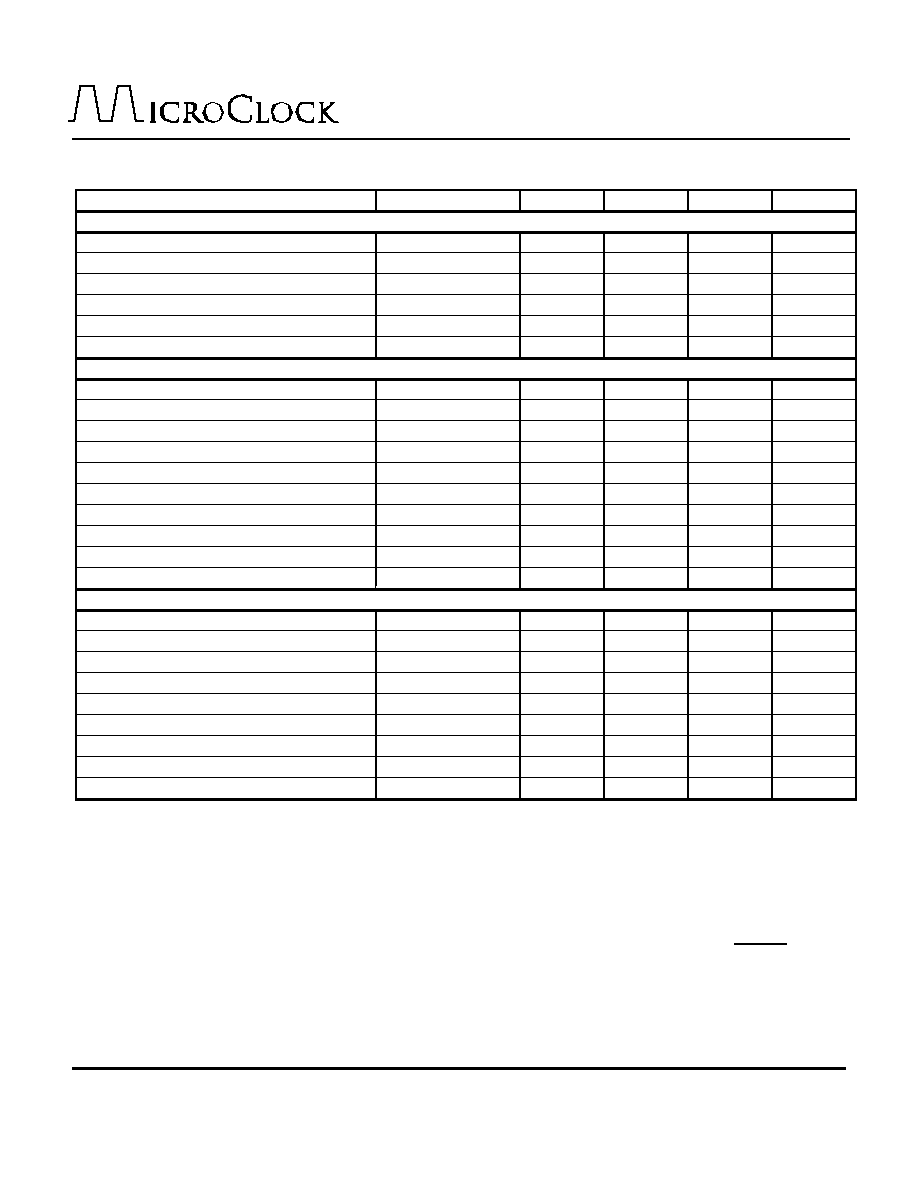
Parameter
Conditions
Minimum
Typical
Maximum
Units
ABSOLUTE MAXIMUM RATINGS (Note 1)
Supply Voltage, VDD
Referenced to GND
7
V
Inputs
Referenced to GND
0.5
VDD+0.5
V
Clock Outputs
Referenced to GND
0.5
VDD+0.5
V
Ambient Operating Temperature
0
70
°C
Soldering Temperature
Max of 10 seconds
260
°C
Storage Temperature
-65
150
°C
DC CHARACTERISTICS (VDD = 5V unless noted)
Operating Voltage, VDD
3.0
5.5
V
Input High Voltage, VIH (INA, INB pins)
VDD-1
VDD/2
V
Input Low Voltage, VIL (INA, INB pins)
VDD/2
1
V
Output High Voltage, 3.3V and 5V
IOH=-8mA
VDD-0.4
V
Output High Voltage, 3.3V and 5V
IOH=-12mA
2.4
V
Output Low Voltage, 3.3V and 5V
IOL=12mA
0.8
V
Operating Supply Current, IDD, at 66.6MHz
No Load
20
mA
Short Circuit Current
Each output
±70
mA
Short Circuit Current at 3.3V
Each output
±35
mA
Input Capacitance
7
pF
AC CHARACTERISTICS (VDD = 5V unless noted)
Input Clock Frequency
67
MHz
Propagation Delay with load=10pF
2
3.5
5
ns
Propagation Delay with load=10pF
At VDD=3.3V
2.5
4.5
6.5
ns
Output Clock Rise Time, 3.3V and 5V
0.8 to 2.0V
1.5
ns
Output Clock Fall Time, 3.3V and 5V
2.0 to 0.8V
1.5
ns
Output Clock Rising Edge Skew, 3.3V and 5V
At VDD/2. Note 2
50
250
ps
Output Clock A to B Skew, 3.3V and 5V
At VDD/2. Note 3
100
500
ps
Maximum load per output pin
At 66.66 MHz
25
pF
Maximum load per side of 7 outputs
Note 4
105
pF
Electrical Specifications
Notes:
1. Stresses beyond those listed under Absolute Maximum Ratings could cause permanent damage to the device. Prolonged exposure
to levels above the operating limits but below the Absolute Maximums may affect device reliability.
2. Between any two A outputs, or any two B outputs, with equal loading.
3. Between any clock A output and any clock B output with INA connected to INB. With VDDA=VDDB and equal loading.
Combined with the 250ps uncertainty of MicroClock’s Clock Synthesizers, this adds to a 750ps total.
4. This is the load sum of all A outputs, or all B outputs, at 66.66MHz. The formula for per side load is CL (F) =
7 x 10⁻³
f (in Hz)
相關(guān)PDF資料 |
PDF描述 |
|---|---|
| MK74ZD133FT | ZD SERIES, PLL BASED CLOCK DRIVER, 32 TRUE OUTPUT(S), 0 INVERTED OUTPUT(S), PDSO56 |
| MK74ZD133FLF | ZD SERIES, PLL BASED CLOCK DRIVER, 32 TRUE OUTPUT(S), 0 INVERTED OUTPUT(S), PDSO56 |
| MK74ZD133FLF | ZD SERIES, PLL BASED CLOCK DRIVER, 32 TRUE OUTPUT(S), 0 INVERTED OUTPUT(S), PDSO56 |
| MK74ZD133F | ZD SERIES, PLL BASED CLOCK DRIVER, 32 TRUE OUTPUT(S), 0 INVERTED OUTPUT(S), PDSO56 |
| MK74ZD133YLFT | ZD SERIES, PLL BASED CLOCK DRIVER, 32 TRUE OUTPUT(S), 0 INVERTED OUTPUT(S), PQFP64 |
相關(guān)代理商/技術(shù)參數(shù) |
參數(shù)描述 |
|---|---|
| MK74CB214RTR | 制造商:ICS 制造商全稱:ICS 功能描述:Dual 1 to 7 Buffalo⑩ Clock Driver |
| MK74CB217 | 制造商:ICS 制造商全稱:ICS 功能描述:Dual 1 to 8 Buffalo⑩ Clock Driver |
| MK74CB217R | 制造商:ICS 制造商全稱:ICS 功能描述:Dual 1 to 8 Buffalo⑩ Clock Driver |
| MK74CB217RTR | 制造商:ICS 制造商全稱:ICS 功能描述:Dual 1 to 8 Buffalo⑩ Clock Driver |
| MK74CB218 | 制造商:ICS 制造商全稱:ICS 功能描述:Dual 1 to 8 Buffalo⑩ Clock Driver |
發(fā)布緊急采購(gòu),3分鐘左右您將得到回復(fù)。