- 您現(xiàn)在的位置:買賣IC網(wǎng) > PDF目錄26831 > MK74ZD133F (INTEGRATED DEVICE TECHNOLOGY INC) ZD SERIES, PLL BASED CLOCK DRIVER, 32 TRUE OUTPUT(S), 0 INVERTED OUTPUT(S), PDSO56 PDF資料下載
參數(shù)資料
| 型號: | MK74ZD133F |
| 廠商: | INTEGRATED DEVICE TECHNOLOGY INC |
| 元件分類: | 時鐘及定時 |
| 英文描述: | ZD SERIES, PLL BASED CLOCK DRIVER, 32 TRUE OUTPUT(S), 0 INVERTED OUTPUT(S), PDSO56 |
| 封裝: | 0.300 INCH, SSOP-56 |
| 文件頁數(shù): | 3/8頁 |
| 文件大小: | 116K |
| 代理商: | MK74ZD133F |
MK74ZD133
PLL and 32-Output Clock Driver
PRELIMINARY
PRELIMINARY INFORMATION
INFORMATION
MDS 74ZD133 C
3
Revision 010899
Printed 11/17/00
Integrated Circuit Systems, Inc.525 Race StreetSan JoseCA95126(408)295-9800telwww.icst.com
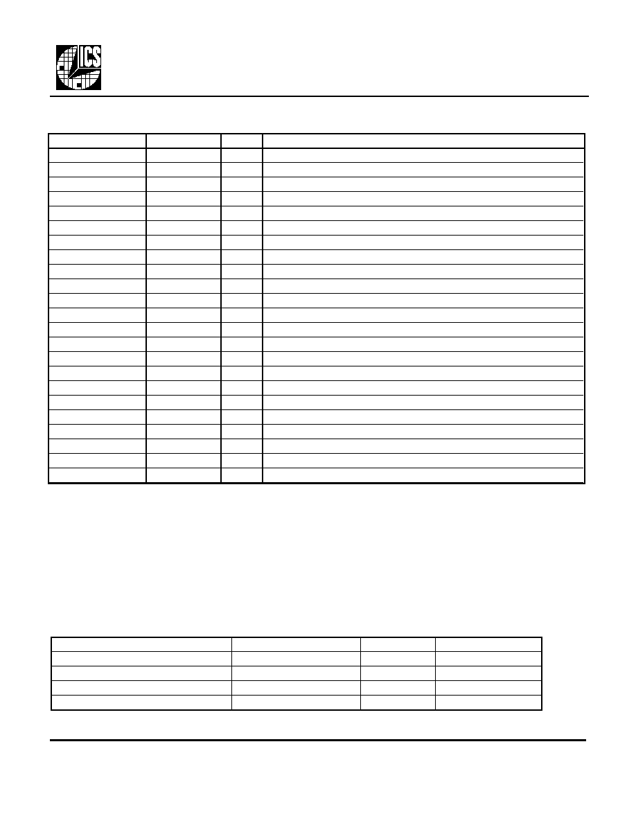
Number
Name
Type
Description
1, 2, 9
OUT1, 2, and 4
O
Clock outputs 1, 2 and 4.
3, 10, 16, 22, 27
GND
P
Connect to ground.
4
CLKIN
I
Clock input for reference.
5
FBIN
I
Feedback input for "zero delay" in Multiplier Mode.
6, 7,28,29,35,36,50,55
VDD
P
Power supply for internal circuits and OUT1:4, OUT15:20, and OUT25:32.
8
FBOUT3
O
Clock output 3. Connect to pin 5 for Zero Delay Mode.
11, 12, 14, 15
OUT5-OUT8
O
Clock outputs 5 through 8; level set by VDD5:8 on pin 13.
13
VDD5:8
P
Power supply for outputs 5 through 8. Cannot exceed VDD.
17, 18, 20, 21
OUT9-OUT12
O
Clock outputs 9 through 12; level set by VDD9:12 on pin 19.
19
VDD9:12
P
Power supply for outputs 9 through 12. Cannot exceed VDD.
23
VDD13:14
P
Power supply for outputs 13 and 14. Cannot exceed VDD.
24
OE (see note)
I
Output Enable. Tri-states all clock outputs when low. Internal pull-up.
25, 26
OUT13-OUT14
O
Clock outputs 13 and 14; level set by VDD13:14 on pin 23.
30, 31, 32, 33, 37, 38 OUT15-OUT20
O
Clock outputs 15 through 20.
34, 39, 45, 51
GND
P
Connect to ground.
40, 41, 43, 44
OUT21-OUT24
O
Clock outputs 21 through 24; level set by VDD21:24 on pin 42.
42
VDD21:24
O
Power supply for outputs 21 through 24. Cannot exceed VDD.
46, 47, 48
OUT25-OUT27
O
Clock outputs 25 through 27.
49
OUT28/S0
I/O
Clock output 28 and output frequency select 0 per table on page 5.
52
OUT29/S1
I/O
Clock output 29 and output frequency select 1 per table on page 5.
53
OUT30/S2
I/O
Clock output 30 and output frequency select 2 per table on page 5.
54
OUT31/S3
I/O
Clock output 31 and output frequency select 3 per table on page 5.
56
OUT32/S4
I/O
Clock output 32 and output frequency select 4 per table on page 5.
Pin Descriptions for 56 pin SSOP (F package)
Type: I = Input, O = output, P = power supply connection, I/O=input upon power up, becoming an output
clock within 10 ms later.
Important Note for OE functionality: To use the output enable function, once the OE has been taken
low, and the outputs have been tri-stated, the VDD must be removed and reapplied for the clocks to run
again.
Staggered output skews for 56 pin SSOP (F) To aid in the reduction of EMI, and to allow the board
designer the flexibility of running different length traces whose clock edges will still line up at their
destinations, the MK74ZD133F comes with different fixed skews for different outputs. All skews are with
respect to OUT1 (pin 1), and are measured into 33
termination resistors with 15 pF capacitive loads.
Output Name
Pin Numbers
Typical Skew
Maximum variation
OUT2, OUT25:32
2, 46:49, 52:54, 56
0
200 ps
OUT4, OUT18:24
9, 33, 37, 38, 40, 41, 43, 44
- 350 ps
200 ps
OUT3, OUT5:8, OUT13:17
8, 11, 12, 14, 15, 25, 26, 30:32
-225 ps
200 ps
OUT9:12
17, 18, 20, 21
-150 ps
200 ps
相關(guān)PDF資料 |
PDF描述 |
|---|---|
| MK74ZD133YLFT | ZD SERIES, PLL BASED CLOCK DRIVER, 32 TRUE OUTPUT(S), 0 INVERTED OUTPUT(S), PQFP64 |
| MK9173-01CS08 | 9173 SERIES, PLL BASED CLOCK DRIVER, 2 TRUE OUTPUT(S), 0 INVERTED OUTPUT(S), PDSO8 |
| MK9173-15CS08 | 9173 SERIES, PLL BASED CLOCK DRIVER, 2 TRUE OUTPUT(S), 0 INVERTED OUTPUT(S), PDSO8 |
| ML6510CQ-130 | PLL BASED CLOCK DRIVER, 8 TRUE OUTPUT(S), 0 INVERTED OUTPUT(S), PQCC44 |
| ML6510CQ-80 | PLL BASED CLOCK DRIVER, 8 TRUE OUTPUT(S), 0 INVERTED OUTPUT(S), PQCC44 |
相關(guān)代理商/技術(shù)參數(shù) |
參數(shù)描述 |
|---|---|
| MK74ZD133FT | 制造商:ICS 制造商全稱:ICS 功能描述:PLL and 32-Output Clock Driver |
| MK74ZD133Y | 制造商:ICS 制造商全稱:ICS 功能描述:PLL and 32-Output Clock Driver |
| MK74ZD133YT | 制造商:ICS 制造商全稱:ICS 功能描述:PLL and 32-Output Clock Driver |
| MK75 | 制造商:Traco Power 功能描述:MOUNTING KIT TIS75 |
| MK7500F | 制造商:Ohmite Mfg Co 功能描述: |
發(fā)布緊急采購,3分鐘左右您將得到回復(fù)。