- 您現(xiàn)在的位置:買賣IC網(wǎng) > PDF目錄377972 > ML6518 (Fairchild Semiconductor Corporation) 18 Line Hot-Insertable Active SCSI Terminator(線熱插入有源SCSI終端器) PDF資料下載
參數(shù)資料
| 型號(hào): | ML6518 |
| 廠商: | Fairchild Semiconductor Corporation |
| 英文描述: | 18 Line Hot-Insertable Active SCSI Terminator(線熱插入有源SCSI終端器) |
| 中文描述: | 18線熱可插入主動(dòng)SCSI端接(線熱插入有源的SCSI終端器) |
| 文件頁數(shù): | 6/8頁 |
| 文件大小: | 84K |
| 代理商: | ML6518 |
ML6518
6
REV. 1.0 10/25/2000
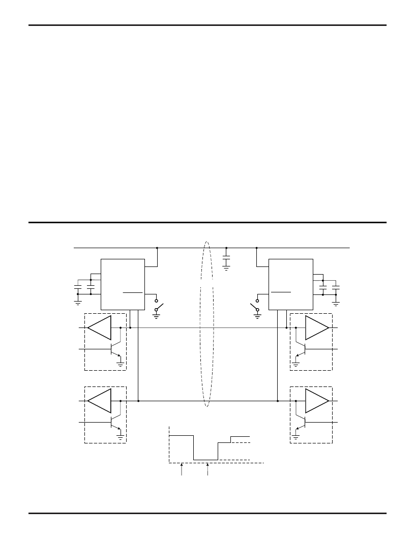
Figure 2. Application Diagram Showing Typical SCSI Bus Configuration with the ML6518
As outlined in Annex G of the ANSI SCSI-3 Parallel
Interface Specification (X3T9.2/855D), “The SCSI bus
termination shall be external to the device being inserted
or removed.” In other words, any terminator connected to
a device being hot inserted/removed should be inactive
(accomplished by grounding the
DISCNKT
pin in the case
of the ML6518). If the terminator being inserted/removed
were in the active state, at some point in time the bus
would be terminated by either 1 or 3 terminators. In either
case, data integrity on the bus will be compromised.
Figure 2 gives an application diagram showing a typical
SCSI bus configuration. To ensure proper operation, the
TERMPWR pin must be connected to the SCSI
TERMPOWER line. Each ML6518 requires parallel 0.1μF
and 10μF capacitors connected between the V
REF
and
GND pins and the TERMPOWER line needs a 10μF
bypass capacitor at one node in the system.
In an 8-bit wide SCSI bus arrangement (“A” Cable),
a single ML6518 would be needed at each end of the SCSI
cable in order to terminate the 18 active signal lines.
16-bit wide SCSI would use one ML6518 and one
ML6599, while 32-bit wide SCSI bus would require two
ML6518s and one ML6599.
In a typical SCSI subsystem, the open collector driver in
the SCSI transceiver pulls low when asserted. The
termination resistance serves as the pull-up when negated.
Figure 2 also shows a typical cable response to a pulse.
The receiving end of the cable will exhibit a single time
delay. When negated, the initial step will reach an
intermediate level (V
STEP
). With higher SCSI data rates,
sampling could occur during this step portion. In order to
get the most noise margin, the step needs to be as high as
possible to prevent false triggering. For this reason the
regulator voltage and the resistor defining the MOSFET
characteristic are trimmed to ensure that the I
O
is as close
as possible to the SCSI maximum current specification.
V
STEP
is defined as:
V
STEP
= V
OL
+ (I
O
∞
Z
O
)
where V
OL
is the driver output low voltage, I
O
is the
current from the receiving terminator, and Z
O
is the
characteristic impedance of the cable.
This is a very important characteristic that the terminator
helps to overcome by increasing the noise margin and
boosting the step as high as possible.
TERMPWR LINE
ML6518
TERMPWR
V
REF
GND
L18
L2 L1
DISCNKT
. . .
0.1μF
10μF
TERMPWR
V
REF
GND
L18
L1 L2
ML6518
DISCNKT
SCSI XCVR
SCSI XCVR
SCSI XCVR
V
REG
V
STEP
V
REG
t
D
t
D
LINE ASSERTED
LINE NEGATED
10μF
0.1μF
10μF
. . .
.
.
V
OL
SCSI CABLE
相關(guān)PDF資料 |
PDF描述 |
|---|---|
| ML65244 | High Speed Dual Quad Buffer/Line Drivers(高速雙通道四緩沖器/線驅(qū)動(dòng)器) |
| ML65L244 | High Speed Dual Quad Buffer/Line Drivers(高速雙通道四緩沖器/線驅(qū)動(dòng)器) |
| ML65245 | High Speed Octal Buffer Transceivers(高速八通道緩沖收發(fā)器) |
| ML65L245 | High Speed Octal Buffer Transceivers(高速八通道緩沖收發(fā)器) |
| ML6553CS-1 | ; Leaded Process Compatible:Yes RoHS Compliant: Yes |
相關(guān)代理商/技術(shù)參數(shù) |
參數(shù)描述 |
|---|---|
| ML6518CH | 制造商:Rochester Electronics LLC 功能描述:- Bulk |
| ML6518CS | 制造商:MICRO-LINEAR 制造商全稱:MICRO-LINEAR 功能描述:18 Line Hot-Insertable Active SCSI Terminator |
| ML65244 | 制造商:MICRO-LINEAR 制造商全稱:MICRO-LINEAR 功能描述:High Speed Dual Quad Buffer/Line Drivers |
| ML65244 WAF | 制造商:Fairchild Semiconductor Corporation 功能描述: |
| ML65244CK | 制造商:MICRO-LINEAR 制造商全稱:MICRO-LINEAR 功能描述:High Speed Dual Quad Buffer/Line Drivers |
發(fā)布緊急采購,3分鐘左右您將得到回復(fù)。