- 您現(xiàn)在的位置:買賣IC網(wǎng) > PDF目錄385617 > MM1268 (MITSUMI ELECTRIC CO LTD) RGB Encoder PDF資料下載
參數(shù)資料
| 型號(hào): | MM1268 |
| 廠商: | MITSUMI ELECTRIC CO LTD |
| 元件分類: | 顏色信號(hào)轉(zhuǎn)換 |
| 英文描述: | RGB Encoder |
| 中文描述: | COLOR SIGNAL ENCODER, PDSO24 |
| 封裝: | SOP-24 |
| 文件頁數(shù): | 6/7頁 |
| 文件大小: | 193K |
| 代理商: | MM1268 |
MITSUMI
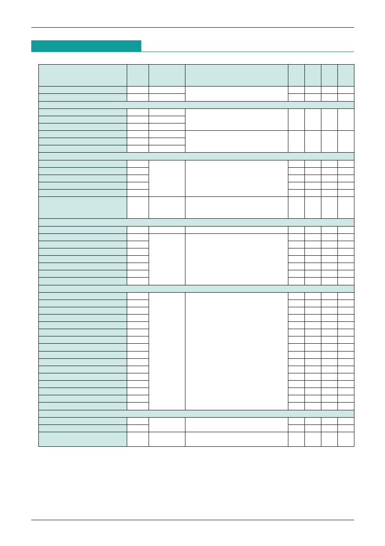
RGB Encoder MM1268
Measurement
circuit
Measurement conditions,
SW conditions
(S1, S2, S3, S4, S5, S6, S7)
V4 : SG6 V5 : SG8
SW conditions (0, 0, 0, 0, 0, 0, 0)
Item
Symbol
Min. Typ. Max. Units
Consumption current 1
Consumption current 2
RGB output characteristics R
OUT
, G
OUT
, B
OUT
R output voltage
G output voltage
B output voltage
Rf characteristic
Gf characteristic
Bf characteristic
Brightness output characteristic Y
OUT
, VIDEO
OUT
Sync level
Red brightness level
Green brightness level
Blue brightness level
White brightness level
I
CC
1
I
CC
2
31
17
40
22
mA
mA
VR
VG
VB
fR
fG
fB
F
E
D
F
E
D
V1, 2, 3 : SG1
SW conditions (1, 1, 0, 0, 1, 1, 0)
0.64 0.71 0.78 V
P
-
P
V1, 2, 3 : SG2/SG1
SW conditions (1, 1, 0, 0, 1, 1, 0)
-
3.0
dB
Y(S)
Y(R)
Y(G)
Y(B)
Y(W)
fY(R)
fY(G)
fY(B)
0.26 0.29 0.33 V
P
-
P
0.17 0.21 0.26
0.35 0.42 0.49
0.065 0.08 0.095
0.6
0.71 0.82
V1 : SG3 V2 : SG4 V3 : SG5
V4 : SG6 V5 : SG8
SW conditions (1, 0, 0, 0, 0, 0, 0)
V
V
V
V
B/C
V1, 2, 3 : SG2/SG1
SW conditions (1, 1, 0, 0, 1, 1, 0)
Brightness f characteristic
B/C
-
3.0
dB
Chroma output characteristic C
OUT
, VIDEO
OUT
NTSC
Burst level
Red level ratio
Red phase
Green level ratio
Green phase
Blue level ratio
Blue phase
PAL
Burst -1 level
Burst -1 phase
Burst -2 level
Burst -2 phase
Red-1 level ratio
Red-1 phase
Red-2 level ratio
Red-2 phase
Green -1 level ratio
Green -1 phase
Green -2 level ratio
Green -2 phase
Blue -1 level ratio
Blue -1 phase
Blue -2 level ratio
Blue -2 phase
NTSC/PAL
Burst position
Burst width
CL(b)
CL(R)
CP(R)
CL(G)
CP(G)
CL(B)
CP(B)
0.2
2.84 3.16 3.48
94
104
2.65 2.95 3.25
231
241
2.01 2.24 2.47
337
347
0.25
0.3
V
P
-
P
V1 : SG3 V2 : SG4 V3 : SG5
V4 : SG6 V5 : SG8
SW conditions (1, 0, 0, 0, 0, 0, 0)
114
deg
A/C
251
deg
357
deg
CL(b1)
CP(b1)
CL(b2)
CP(b2)
CL(R1)
CP(R1)
CL(R2)
CP(R2)
CL(G1)
CP(G1)
CL(G2)
CP(G2)
CL(B1)
CP(B1)
CL(B2)
CP(B2)
0.2
125
0.2
215
2.84 3.16 3.48
94
104
2.84 3.16 3.48
246
256
2.65 2.95 3.25
231
241
2.65 2.95 3.25
109
119
2.01 2.24 2.47
337
347
2.01 2.24 2.47
3
13
0.25
135
0.25
225
0.3
145
0.3
235
V
P
-
P
deg
V
P
-
P
deg
114
deg
V1 : SG3 V2 : SG4 V3 : SG5
V4 : SG6 V5 : SG8
SW conditions (1, 0, 0, 1, 0, 0, 1)
A/C
266
deg
251
deg
129
deg
357
deg
23
deg
td
tw
VL
A/C
V1 : SG3 V2 : SG4 V3 : SG5 V4 : SG6
SW conditions (1, 0, 0, 1, 0, 0, 1)
V1~3 : no signal, V4 : SG6
SW conditions (1, 0, 0, 1, 0, 0, 1)
0.4
2.5
0.6
2.75
0.75
3.2
20
μS
μS
Carrier lea
A/C
mV
P
-
P
Electrical Characteristics
(Ta=25°C, V
CC
=1, 2=5V)
相關(guān)PDF資料 |
PDF描述 |
|---|---|
| MM1270 | Low-Output Voltage Low-Saturation Three-Pin Regulator |
| MM1278 | High Precision Operational Amplifier |
| MM1285 | Hybrid Driver Monolithic IC |
| MM1288CQ | TFT Liquid Crystal Interface |
| MM1291AF | Protection of Lithium Ion Batteries (one cell) |
相關(guān)代理商/技術(shù)參數(shù) |
參數(shù)描述 |
|---|---|
| MM1270 | 制造商:MITSUMI 制造商全稱:Mitsumi Electronics, Corp. 功能描述:Low-Output Voltage Low-Saturation Three-Pin Regulator |
| MM1272F | 制造商:Ohmite Mfg Co 功能描述: |
| MM1278 | 制造商:MITSUMI 制造商全稱:Mitsumi Electronics, Corp. 功能描述:High Precision Operational Amplifier |
| MM1285 | 制造商:MITSUMI 制造商全稱:Mitsumi Electronics, Corp. 功能描述:Hybrid Driver Monolithic IC |
| MM1288CQ | 制造商:MITSUMI 制造商全稱:Mitsumi Electronics, Corp. 功能描述:TFT Liquid Crystal Interface |
發(fā)布緊急采購,3分鐘左右您將得到回復(fù)。