- 您現(xiàn)在的位置:買賣IC網(wǎng) > PDF目錄377976 > MM74C911 (Fairchild Semiconductor Corporation) Simplified Multi-Digit LED Display Controller(多數(shù)字式LED顯示控制器) PDF資料下載
參數(shù)資料
| 型號: | MM74C911 |
| 廠商: | Fairchild Semiconductor Corporation |
| 英文描述: | Simplified Multi-Digit LED Display Controller(多數(shù)字式LED顯示控制器) |
| 中文描述: | 簡化的多位LED顯示控制器(多數(shù)字式的LED顯示控制器) |
| 文件頁數(shù): | 2/26頁 |
| 文件大小: | 639K |
| 代理商: | MM74C911 |
第1頁當(dāng)前第2頁第3頁第4頁第5頁第6頁第7頁第8頁第9頁第10頁第11頁第12頁第13頁第14頁第15頁第16頁第17頁第18頁第19頁第20頁第21頁第22頁第23頁第24頁第25頁第26頁
By raising the Digit In-Out (DIO) input high, the internal oscil-
lator is disabled and the digit outputs become inputs which
control reading of the 4-digit latches. This allows the
MM74C911 to be slaved to other multiplex timing signals. If
both SOE and DIO are held high, both the display and oscil-
lator are disabled causing the MM74C911 to be in a
low-power mode where it typically draws less than 1 μA. Fig-
ure 3 shows the truth table for these control inputs.
III. FUNCTIONAL DESCRIPTION—
MM74C912/MM74C917
The functional block diagram for the MM74C912 and
MM74C917 is shown in Figure 4 These devices are very
similar to the MM74C911. There are only five data inputs on
the MM74C912 and MM74C917 which are buffered, then
bussed to six 5-bit dual-port latches. The address present on
K1, K2, and K3 will dictate which of the six latches will be
loaded when both CE and WE are low. The outputs of all of
the latches are commonly bussed and fed into a decoder
ROM which converts BCD (MM74C912) or hexadecimal
(MM74C917) code to seven segment. The fifth bit is the
decimal point, which bypasses the ROM. The 8-segment bits
are then buffered by eight NPN-segment drivers. Like the
MM74C911, these outputs are 3-STATE and will blank the
display when SOE is held high.
All of the multiplexing is controlled by an internal oscillator
and control logic. The logic sequentially reads each latch
and activates the digit outputs. The oscillator can be dis-
abled by raising the Oscillator Enable (OSE ) input high, but
the digit outputs do not become inputs and thus the
MM74C912, and MM74C917 can not be slaved. However,
by raising both SOE and OSE high, these parts can be put
into a low-power mode similar to the MM74C911. Figure 3
shows the controller operating modes.
The MM74C912 and the MM74C917 are identical except for
the last seven ROM locations. The ROM outputs are shown
in Figure 5 for both parts.
IV. DISPLAY INTERFACE DESIGN
A. Common Cathode LED’s
Since the MM74C911/MM74C912/MM74C917 contain all
the multiplex circuitry necessary to operate a 4- or 6-digit dis-
play, all the designer must do is choose appropriate segment
resistors and digit drivers to properly illuminate the LEDs. A
typical LED connection is shown in Figure 6 Based on the
selected display, a certain segment current will be required.
This current will determine the value of the segment resistor
and the type of digit driver necessary. The design for the
MM74C911 is nearly the same as for the MM74C912/
MM74C917 except that due to multiplexing the 6-digit con-
trollers must be designed to a higher peak current value.
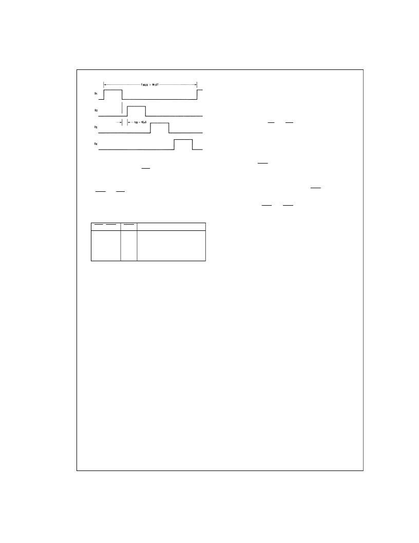
AN006030-2
FIGURE 2. MUX Timing for MM74C911
DIO /OSE
0
0
1
1
SOE
0
1
0
1
Mode
NORMAL DISPLAY MODE
DISPLAY BLANKED
WILL DISPLAY ONE DIGIT
*
LOW POWER MODE
FIGURE 3. Operating Modes for the
MM74C911/MM74C912/MM74C917
(
*
The 74C911 Digit Outputs become Inputs)
www.fairchildsemi.com
2
相關(guān)PDF資料 |
PDF描述 |
|---|---|
| MM74C912 | Simplified Multi-Digit LED Display Controller(多數(shù)字式LED顯示控制器) |
| MM74C917 | Simplified Multi-Digit LED Display Controller(多數(shù)字式LED顯示控制器) |
| MM74C912N | 6-Digit BCD Display Controller/Driver |
| MM74C914 | Hex Schmitt Trigger with Extended Input Voltage |
| MM74C914M | Hex Schmitt Trigger with Extended Input Voltage |
相關(guān)代理商/技術(shù)參數(shù) |
參數(shù)描述 |
|---|---|
| MM74C911N | 功能描述:LED顯示驅(qū)動器 4-Dgt Dis Controller RoHS:否 制造商:Micrel 數(shù)位數(shù)量:5 片段數(shù)量: 安裝風(fēng)格:SMD/SMT 封裝 / 箱體:PLCC-44 工作電源電壓:4.75 V to 11 V 最大電源電流:10 mA 最大工作溫度:+ 85 C 最小工作溫度:- 40 C 封裝:Tube |
| MM74C912 | 制造商:FAIRCHILD 制造商全稱:Fairchild Semiconductor 功能描述:6-Digit BCD Display Controller/Driver |
| MM74C912N | 功能描述:LED顯示驅(qū)動器 6-Dgt BCD Dis Con/Dr RoHS:否 制造商:Micrel 數(shù)位數(shù)量:5 片段數(shù)量: 安裝風(fēng)格:SMD/SMT 封裝 / 箱體:PLCC-44 工作電源電壓:4.75 V to 11 V 最大電源電流:10 mA 最大工作溫度:+ 85 C 最小工作溫度:- 40 C 封裝:Tube |
| MM74C914 | 制造商:FAIRCHILD 制造商全稱:Fairchild Semiconductor 功能描述:Hex Schmitt Trigger with Extended Input Voltage |
| MM74C914J | 制造商:NSC 制造商全稱:National Semiconductor 功能描述:Hex Schmitt Trigger with Extended Input Voltage |
發(fā)布緊急采購,3分鐘左右您將得到回復(fù)。