- 您現(xiàn)在的位置:買賣IC網(wǎng) > PDF目錄377977 > MM74HC04N (FAIRCHILD SEMICONDUCTOR CORP) CERAMIC CHIP/MIL-PRF-55681 PDF資料下載
參數(shù)資料
| 型號(hào): | MM74HC04N |
| 廠商: | FAIRCHILD SEMICONDUCTOR CORP |
| 元件分類: | 通用總線功能 |
| 英文描述: | CERAMIC CHIP/MIL-PRF-55681 |
| 中文描述: | HC/UH SERIES, HEX 1-INPUT INVERT GATE, PDIP14 |
| 封裝: | 0.300 INCH, PLASTIC, MS-001, DIP-14 |
| 文件頁數(shù): | 1/7頁 |
| 文件大?。?/td> | 81K |
| 代理商: | MM74HC04N |
2005 Fairchild Semiconductor Corporation
DS005069
www.fairchildsemi.com
September 1983
Revised January 2005
M
MM74HC04
Hex Inverter
General Description
The MM74HC04 inverters utilize advanced silicon-gate
CMOS technology to achieve operating speeds similar to
LS-TTL gates with the low power consumption of standard
CMOS integrated circuits.
The MM74HC04 is a triple buffered inverter. It has high
noise immunity and the ability to drive 10 LS-TTL loads.
The 74HC logic family is functionally as well as pin-out
compatible with the standard 74LS logic family. All inputs
are protected from damage due to static discharge by inter-
nal diode clamps to V
CC
and ground.
Features
I
Typical propagation delay: 8 ns
I
Fan out of 10 LS-TTL loads
I
Quiescent power consumption: 10
μ
W maximum at
room temperature
I
Low input current: 1
μ
A maximum
Ordering Code:
Devices also available in Tape and Reel. Specify by appending the suffix letter “X” to the ordering code.
Pb-Free package per JEDEC J-STD-020B.
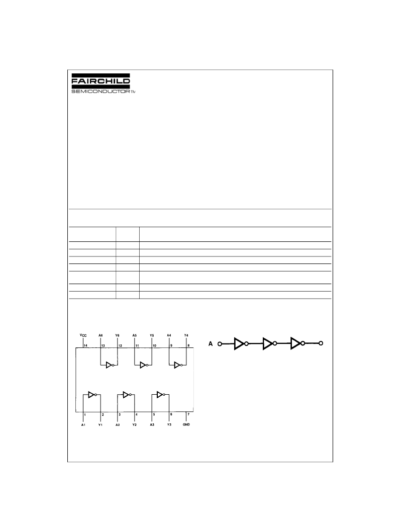
Connection Diagram
Pin Assignments for DIP, SOIC, SOP and TSSOP
Top View
Logic Diagram
1 of 6 Inverters
Order Number
Package
Number
M14A
Package Description
MM74HC04M
MM74HC04M_NL
MM74HC04SJ
MM74HC04MTC
MM74HC04MTC_NL
14-Lead Small Outline Integrated Circuit (SOIC), JEDEC MS-012, 0.150" Narrow
Pb-Free 14-Lead Small Outline Integrated Circuit (SOIC), JEDEC MS-012, 0.150" Narrow
Pb-Free 14-Lead Small Outline Package (SOP), EIAJ TYPE II, 5.3mm Wide
14-Lead Thin Shrink Small Outline Package (TSSOP), JEDEC MO-153, 4.4mm Wide
Pb-Free 14-Lead Thin Shrink Small Outline Package (TSSOP), JEDEC MO-153, 4.4mm
Wide
14-Lead Plastic Dual-In-Line Package (PDIP), JEDEC MS-001, 0.300" Wide
Pb-Free 14-Lead Plastic Dual-In-Line Package (PDIP), JEDEC MS-001, 0.300" Wide
M14D
MTC14
MTC14
MM74HC04N
MM74HC04N_NL
N14A
N14A
相關(guān)PDF資料 |
PDF描述 |
|---|---|
| MM74HC04SJ | CERAMIC CHIP/MIL-PRF-55681 |
| MM74HC08 | Quad 2-Input AND Gate |
| MM74HC08M | Quad 2-Input AND Gate |
| MM74HC08N | Quad 2-Input AND Gate |
| MM74HC08SJ | Quad 2-Input AND Gate |
相關(guān)代理商/技術(shù)參數(shù) |
參數(shù)描述 |
|---|---|
| MM74HC04N | 制造商:Fairchild Semiconductor Corporation 功能描述:IC GATES/INVERTERS LOGIC ROHS COMPLIANT |
| MM74HC04N | 制造商:Fairchild Semiconductor Corporation 功能描述:IC 74HC CMOS 74HC04 DIP14 6V |
| MM74HC04N/A+ | 制造商:未知廠家 制造商全稱:未知廠家 功能描述:Hex Inverter |
| MM74HC04N/B+ | 制造商:未知廠家 制造商全稱:未知廠家 功能描述:Hex Inverter |
| MM74HC04N_NL | 制造商:FAIRCHILD 制造商全稱:Fairchild Semiconductor 功能描述:Hex Inverter |
發(fā)布緊急采購,3分鐘左右您將得到回復(fù)。