- 您現(xiàn)在的位置:買賣IC網(wǎng) > PDF目錄359177 > MMA7450L (飛思卡爾半導(dǎo)體(中國(guó))有限公司) 【2g/【4g/【8g Three Axis Low-g Digital Output Accelerometer PDF資料下載
參數(shù)資料
| 型號(hào): | MMA7450L |
| 廠商: | 飛思卡爾半導(dǎo)體(中國(guó))有限公司 |
| 英文描述: | 【2g/【4g/【8g Three Axis Low-g Digital Output Accelerometer |
| 中文描述: | 【2克/【4克/【八克三三軸低g加速度計(jì)的數(shù)字輸出 |
| 文件頁(yè)數(shù): | 8/22頁(yè) |
| 文件大小: | 389K |
| 代理商: | MMA7450L |
第1頁(yè)第2頁(yè)第3頁(yè)第4頁(yè)第5頁(yè)第6頁(yè)第7頁(yè)當(dāng)前第8頁(yè)第9頁(yè)第10頁(yè)第11頁(yè)第12頁(yè)第13頁(yè)第14頁(yè)第15頁(yè)第16頁(yè)第17頁(yè)第18頁(yè)第19頁(yè)第20頁(yè)第21頁(yè)第22頁(yè)

Sensors
8
Freescale Semiconductor
MMA7450L
DIGITAL INTERFACE
The MMA7450L has both an I
2
C and SPI digital output
available for a communication interface. When CS pin is used
for Slave Select, SPI communication is selected. When CS is
high, I
2
C communication is selected and SPI is disabled.
NOTE:
It is recommended to disable I
2
C during SPI
communication to avoid communication
errors between devices using a different SPI
communication protocol. To disable I
2
C, set
the I
2
CDIS bit in I
2
C Device Address register
using SPI.
I
2
C SLAVE INTERFACE
I
2
C is a synchronous serial communication between a
master device and one or more slave devices. The master is
typically a microcontroller, which provides the serial clock
signal and addresses the slave device(s) on the bus. The
MMA7450L communicates only in slave operation where the
device address is $1D. Multiple read and write modes are
available. The protocol supports slave only operation. It does
not support Hs mode, “10-bit addressing”, “general call” and
:”START byte”.
SINGLE BYTE READ
The MMA7450L has an 8-bit ADC that can sample,
convert and return sensor data on request. The transmission
of an 8-bit command begins on the falling edge of SCL. After
the eight clock cycles are used to send the command, note
that the data returned is sent with the MSB first once the data
is received.
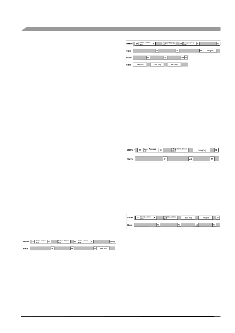
Figure 7
shows the timing diagram for the
accelerometer 8-bit I
2
C read operation. The Master (or MCU)
transmits a start condition (S) to the MMA7450L, slave
address ($1D), with the R/W bit set to “0” for a write, and the
MMA7450L sends an acknowledgement. Then the Master (or
MCU) transmits the 8-bit address of the register to read and
the MMA7450L sends an acknowledgement. The Master (or
MCU) transmits a repeated start condition (SR) and then
addresses the MMA7450L ($1D) with the R/W bit set to “1” for
a read from the previously selected register. The Slave then
acknowledges and transmits the data from the requested
register. The Master does not acknowledge (NACK) it
received the transmitted data, but transmits a stop condition
to end the data transfer.
Figure 7. Single Byte Read - The Master is reading one
address from the MMA7450L
MULTIPLE BYTES READ
The MMA7450L automatically increments the received
register address commands after a read command is
received. Therefore, after following the steps of a single byte
read, multiple bytes of data can be read from sequential
registers after each MMA7450L acknowledgment (ACK) is
received until a NACK is received from the Master followed
by a stop condition (SP) signalling an end of transmission.
See
Figure 8
.
Figure 8. Multiple Bytes Read - The Master is reading
multiple sequential registers from the MMA7450L
SINGLE BYTE WRITE
To start a write command, the Master transmits a start
condition (ST) to the MMA7450L, slave address ($1D) with
the R/W bit set to “0” for a write, the MMA7450L sends an
acknowledgement. Then the Master (MCU) transmits the 8-
bit address of the register to write to, and the MMA7450L
sends an acknowledgement. Then the Master (or MCU)
transmits the 8-bit data to write to the designated register and
the MMA7450L sends an acknowledgement that it has
received the data. Since this transmission is complete, the
Master transmits a stop condition (SP) to the data transfer.
The data sent to the MMA7450L is now stored in the
appropriate register. See
Figure 9
.
Figure 9. Single Byte Write - The Master (MCU) is writing
to a single register of the MMA7450L
MULTIPLE BYTES WRITE
The MMA7450L automatically increments the received
register address commands after a write command is
received. Therefore, after following the steps of a single byte
write, multiple bytes of data can be written to sequential
registers after each MMA7450L acknowledgment (ACK) is
received. See
Figure 10
.
Figure 10. Multiple Byte Writes - The Master (MCU) is
writing to multiple sequential registers of the MMA7450L
SPI SLAVE INTERFACE
The MMA7450L also uses serial peripheral interface
communication as a digital communication. The SPI
communication is primarily used for synchronous serial
communication between a master device and one or more
slave devices. See
Figure 16
for an example of how to
configure one master with two MMA7450L devices. The
MMA7450L is always operated as a slave device. Typically,
the master device would be a microcontroller which would
drive the clock (SPC) and chip select (CS) signals.
The SPI interface consists of two control lines and two data
lines: CS, SPC, SDI, and SDO. The CS, also known as Chip
Select, is the slave device enable which is controlled by the
SPI master. CS is driven low at the start of a transmission. CS
相關(guān)PDF資料 |
PDF描述 |
|---|---|
| MMA7455L | Three Axis Low-g Digital Output Accelerometer |
| MMBD4148T | 0.15 A, 75 V, SILICON, SIGNAL DIODE |
| MMBFJ309L | TRANSISTOR | JFET | N-CHANNEL | 30MA I(DSS) | SOT-23 |
| MMBT2222A | SMALL SIGNAL NPN TRANSISTOR |
| MMBT2222A | NPN General Purpose Amplifier |
相關(guān)代理商/技術(shù)參數(shù) |
參數(shù)描述 |
|---|---|
| MMA7450LR1 | 制造商:FREESCALE 制造商全稱:Freescale Semiconductor, Inc 功能描述:【2g/【4g/【8g Three Axis Low-g Digital Output Accelerometer |
| MMA7450LR2 | 制造商:FREESCALE 制造商全稱:Freescale Semiconductor, Inc 功能描述:【2g/【4g/【8g Three Axis Low-g Digital Output Accelerometer |
| MMA7450LT | 制造商:Freescale Semiconductor 功能描述:ACCELEROMETER TRIPLE ?2G/?4G/?8G 2.8V 14-PIN LGA TRAY - Trays |
| MMA7455L | 制造商:FREESCALE 制造商全稱:Freescale Semiconductor, Inc 功能描述:±2g/±4g/±8g Three Axis Low-g Digital Output Accelerometer |
| MMA7455L_08 | 制造商:FREESCALE 制造商全稱:Freescale Semiconductor, Inc 功能描述:±2g/±4g/±8g Three Axis Low-g Digital Output Accelerometer |
發(fā)布緊急采購(gòu),3分鐘左右您將得到回復(fù)。