- 您現(xiàn)在的位置:買(mǎi)賣(mài)IC網(wǎng) > PDF目錄385629 > MMSZ4693ET1 (ON SEMICONDUCTOR) Zener Voltage Regulators(齊納穩(wěn)壓管) PDF資料下載
參數(shù)資料
| 型號(hào): | MMSZ4693ET1 |
| 廠商: | ON SEMICONDUCTOR |
| 元件分類(lèi): | 參考電壓二極管 |
| 英文描述: | Zener Voltage Regulators(齊納穩(wěn)壓管) |
| 中文描述: | 7.5 V, 0.5 W, SILICON, UNIDIRECTIONAL VOLTAGE REGULATOR DIODE |
| 封裝: | PLASTIC, CASE 425-04, 2 PIN |
| 文件頁(yè)數(shù): | 1/5頁(yè) |
| 文件大小: | 72K |
| 代理商: | MMSZ4693ET1 |
Semiconductor Components Industries, LLC, 2005
August, 2005 Rev. 4
1
Publication Order Number:
MMSZ4678ET1/D
MMSZ4678ET1 Series
Zener Voltage Regulators
500 mW SOD123 Surface Mount
Three complete series of Zener diodes are offered in the convenient,
surface mount plastic SOD123 package. These devices provide a
convenient alternative to the leadless 34package style.
Features
500 mW Rating on FR4 or FR5 Board
Wide Zener Reverse Voltage Range 1.8 V to 43 V
Package Designed for Optimal Automated Board Assembly
Small Package Size for High Density Applications
ESD Rating of Class 3 (>16 kV) per Human Body Model
Peak Power 225 W (8 x 20 s)
PbFree Packages are Available
Mechanical Characteristics:
CASE:
Void-free, transfer-molded, thermosetting plastic case
FINISH:
Corrosion resistant finish, easily solderable
MAXIMUM CASE TEMPERATURE FOR SOLDERING PURPOSES:
260
°
C for 10 Seconds
POLARITY:
Cathode indicated by polarity band
FLAMMABILITY RATING:
UL 94 V0
MAXIMUM RATINGS
Rating
Symbol
Max
Unit
Peak Power Dissipation @ 20 s (Note 1)
@ T
L
≤
25
°
C
P
pk
225
W
Total Power Dissipation on FR5 Board,
(Note 2) @ T
L
= 75
°
C
Derated above 75
°
C
P
D
500
6.7
mW
mW/
°
C
Thermal Resistance, (Note 3)
JunctiontoAmbient
R
JA
340
°
C/W
Thermal Resistance, (Note 3)
JunctiontoLead
R
JL
150
°
C/W
Junction and Storage Temperature Range
T
J
, T
stg
55 to
+150
°
C
Maximum ratings are those values beyond which device damage can occur.
Maximum ratings applied to the device are individual stress limit values (not
normal operating conditions) and are not valid simultaneously. If these limits are
exceeded, device functional operation is not implied, damage may occur and
reliability may be affected.
1. Nonrepetitive current pulse per Figure 11.
2. FR5 = 3.5 x 1.5 inches, using the minimum recommended footprint.
3. Thermal Resistance measurement obtained via infrared Scan Method.
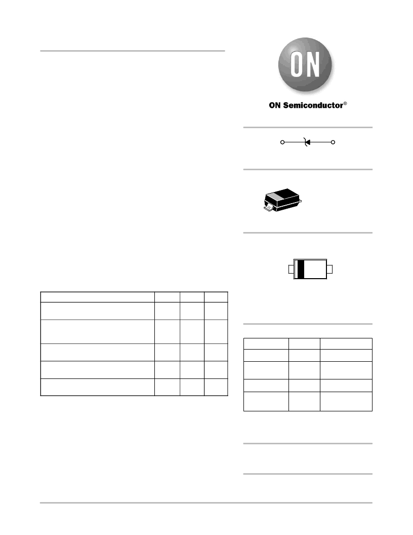
SOD123
CASE 425
STYLE 1
1
Cathode
2
Anode
See specific marking information in the device marking
column of the Electrical Characteristics table on page 2 of
this data sheet.
DEVICE MARKING INFORMATION
1
2
Devices listed in
bold, italic
are ON Semiconductor
Preferred
devices.
Preferred
devices are recommended
choices for future use and best overall value.
http://onsemi.com
MARKING DIAGRAM
xxx = Device Code (Refer to page 2)
M
= Date Code
= PbFree Package
(Note: Microdot may be in either location)
xxx M
1
Device
Package
Shipping
ORDERING INFORMATION
MMSZ4xxxET1
SOD123
3000/Tape & Reel
MMSZ4xxxET3
SOD123
10000/Tape & Reel
For information on tape and reel specifications,
including part orientation and tape sizes, please
refer to our Tape and Reel Packaging Specifications
Brochure, BRD8011/D.
MMSZ4xxxET1G
SOD123
(PbFree)
3000/Tape & Reel
MMSZ4xxxET3G
SOD123
(PbFree)
10000/Tape & Reel
相關(guān)PDF資料 |
PDF描述 |
|---|---|
| MMSZ4711ET1 | Zener Voltage Regulators(齊納穩(wěn)壓管) |
| MMSZ4691ET1 | Zener Voltage Regulators(齊納穩(wěn)壓管) |
| MMSZ4678ET1 | Zener Voltage Regulators(齊納穩(wěn)壓管) |
| MMSZ4684ET1 | Zener Voltage Regulators(齊納穩(wěn)壓管) |
| MMSZ4688ET1 | Zener Voltage Regulators(齊納穩(wěn)壓管) |
相關(guān)代理商/技術(shù)參數(shù) |
參數(shù)描述 |
|---|---|
| MMSZ4693ET1G | 制造商:ONSEMI 制造商全稱(chēng):ON Semiconductor 功能描述:Zener Voltage Regulators 500 mW SOD−123 Surface Mount |
| MMSZ4693ET3 | 制造商:ONSEMI 制造商全稱(chēng):ON Semiconductor 功能描述:Zener Voltage Regulators 500 mW SOD−123 Surface Mount |
| MMSZ4693ET3G | 制造商:ONSEMI 制造商全稱(chēng):ON Semiconductor 功能描述:Zener Voltage Regulators 500 mW SOD−123 Surface Mount |
| MMSZ4693-F | 制造商:TAITRON 制造商全稱(chēng):TAITRON Components Incorporated 功能描述:500mW Two Terminals SMD Zener Diodes |
| MMSZ4693-HE3-08 | 制造商:Vishay Semiconductors 功能描述: 制造商:Vishay Intertechnologies 功能描述:ZENER DIODE SOD123 |
發(fā)布緊急采購(gòu),3分鐘左右您將得到回復(fù)。