- 您現(xiàn)在的位置:買賣IC網(wǎng) > PDF目錄383627 > MMT08B350T3G (ON SEMICONDUCTOR) Thyristor Surge Protectors High Voltage Bidirectional TSPD PDF資料下載
參數(shù)資料
| 型號: | MMT08B350T3G |
| 廠商: | ON SEMICONDUCTOR |
| 元件分類: | 浪涌電流限制器 |
| 英文描述: | Thyristor Surge Protectors High Voltage Bidirectional TSPD |
| 中文描述: | 400 V, 32 A, SILICON SURGE PROTECTOR, DO-214AA |
| 封裝: | CASE 403C, SMT, SMB, 2 PIN |
| 文件頁數(shù): | 2/5頁 |
| 文件大小: | 65K |
| 代理商: | MMT08B350T3G |
MMT08B350T3
http://onsemi.com
2
THERMAL CHARACTERISTICS
Characteristic
Symbol
Max
Unit
Operating Temperature Range Blocking or Conducting State
T
J1
40 to +125
°
C
Overload Junction Temperature Maximum Conducting State Only
T
J2
+175
°
C
Maximum Lead Temperature for Soldering Purposes 1/8
″
from Case for 10 Seconds
T
L
260
°
C
ELECTRICAL CHARACTERISTICS
(T
J
= 25
°
C unless otherwise noted) Devices are bidirectional. All electrical parameters apply to
forward and reverse polarities.
Characteristics
Symbol
Min
Typ
Max
Unit
Breakover Voltage (Both polarities)
(dv/dt = 100 V/ s, I
SC
= 1.0 A, Vdc = 1000 V)
(+65
°
C)
V
(BO)
400
412
V
Breakover Voltage (Both polarities)
(f = 60 Hz, I
SC
= 1.0 A(rms), V
OC
= 1000 V(rms),
R
I
= 1.0 k , t = 0.5 cycle) (Note 3)
(+65
°
C)
V
(BO)
400
412
V
Breakover Voltage Temperature Coefficient
dV
(BO)
/dT
J
0.12
V/
°
C
Breakdown Voltage (I
(BR)
= 1.0 mA) Both polarities
V
(BR)
350
V
Off State Current (V
D1
= 50 V) Both polarities
Off State Current
(V
D2
= V
DM
) Both polarities
I
D1
I
D2
2.0
5.0
A
OnState Voltage (I
T
= 1.0 A)
(PW
≤
300 s, Duty Cycle
≤
2%) (Note 3)
V
T
1.7
3.0
V
Breakover Current (f = 60 Hz, V
DM
= 1000 V(rms), R
S
= 1.0 k )
Both polarities
I
BO
475
mA
Holding Current (Both polarities) (Note 3)
V
S
= 500 V; I
T
(Initiating Current) =
1.0 A (+65
°
C)
I
H
150
130
270
mA
Critical Rate of Rise of OffState Voltage
(Linear waveform, V
D
= Rated V
BR
, T
J
= 25
°
C)
dv/dt
2000
V/ s
Capacitance (f = 1.0 MHz, 50 Vdc, 1.0 V rms Signal)
Capacitance
(f = 1.0 MHz, 2.0 Vdc, 1.0 V rms Signal)
C
O
20
42
25
45
pF
3. Measured under pulse conditions to reduce heating.
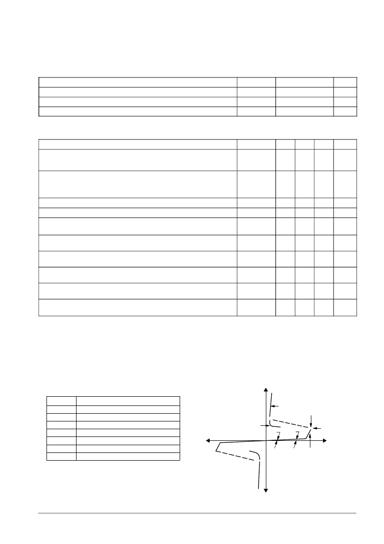
+ Current
+ Voltage
V
TM
V
(BO)
I
(BO)
I
D2
I
D1
V
D1
V
D2
V
(BR)
I
H
Symbol
I
D1
, I
D2
V
D1
, V
D2
V
BR
V
BO
I
BO
I
H
V
TM
Parameter
Off State Leakage Current
Off State Blocking Voltage
Breakdown Voltage
Breakover Voltage
Breakover Current
Holding Current
On State Voltage
Voltage Current Characteristic of TSPD
(Bidirectional Device)
相關(guān)PDF資料 |
PDF描述 |
|---|---|
| MMT10B350T3 | Thyristor Surge Protectors High Voltage Bidirectional TSPD |
| MMT10B350T3G | Thyristor Surge Protectors High Voltage Bidirectional TSPD |
| MMUN2134 | Bias Resistor Transistor |
| MMVL109T1 | Silicon Epicap Diode |
| MMVL2101T1 | Silicon Tuning Diode |
相關(guān)代理商/技術(shù)參數(shù) |
參數(shù)描述 |
|---|---|
| MMT100J224 | 制造商:Nissei Electronics 功能描述: |
| MMT100J684 | 制造商:Nissei Electronics 功能描述: |
| MMT-102-01-F-DH | 制造商:Samtec Inc 功能描述:2MM SMT STRIPS - Bulk |
| MMT-102-01-F-DH-A | 制造商:Samtec Inc 功能描述:2MM SMT STRIPS - Bulk |
| MMT-102-01-F-DH-LC | 制造商:Samtec Inc 功能描述:2MM SMT STRIPS - Bulk |
發(fā)布緊急采購,3分鐘左右您將得到回復(fù)。