- 您現(xiàn)在的位置:買賣IC網(wǎng) > PDF目錄359183 > MOC8101 (VISHAY SEMICONDUCTORS) Optocoupler DC-IN 1-CH Transistor DC-OUT 6-Pin PDIP PDF資料下載
參數(shù)資料
| 型號: | MOC8101 |
| 廠商: | VISHAY SEMICONDUCTORS |
| 元件分類: | 光電耦合器 |
| 英文描述: | Optocoupler DC-IN 1-CH Transistor DC-OUT 6-Pin PDIP |
| 中文描述: | Transistor Output Optocouplers Phototransistor Out Single CTR 50-80% |
| 文件頁數(shù): | 2/8頁 |
| 文件大?。?/td> | 164K |
| 代理商: | MOC8101 |
MOC8101, MOC8102, MOC8103, MOC8104, MOC8105
www.vishay.com
Vishay Semiconductors
Rev. 1.6, 13-Sep-11
2
Document Number: 83660
For technical questions, contact:
optocoupleranswers@vishay.com
THIS DOCUMENT IS SUBJECT TO CHANGE WITHOUT NOTICE. THE PRODUCTS DESCRIBED HEREIN AND THIS DOCUMENT
ARE SUBJECT TO SPECIFIC DISCLAIMERS, SET FORTH AT
www.vishay.com/doc91000
Notes
Stresses in excess of the absolute maximum ratings can cause permanent damage to the device. Functional operation of the device is not
implied at these or any other conditions in excess of those given in the operational sections of this document. Exposure to absolute
maximum ratings for extended periods of the time can adversely affect reliability.
(1)
Refer to reflow profile for soldering conditions for surface mounted devices (SMD). Refer to wave profile for soldering conditions for through
hole devices (DIP).
(2)
Applies to wide bending option 6.
Note
Minimum and maximum values are testing requirements. Typical values are characteristics of the device and are the result of engineering
evaluation. Typical values are for information only and are not part of the testing requirements.
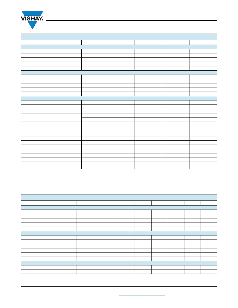
ABSOLUTE MAXIMUM RATINGS
(T
amb
= 25 °C, unless otherwise specified)
PARAMETER
INPUT
Reverse voltage
Forward continuous current
Surge forward current
Power dissipation
Derate linearly from 25°C
OUTPUT
Collector emitter breakdown voltage
Emitter collector breakdown voltage
Collector current
Derate linearly from 25°C
Power dissipation
COUPLER
Isolation test voltage
TEST CONDITION
SYMBOL
VALUE
UNIT
V
R
I
F
I
FSM
P
diss
6.0
60
2.5
100
1.33
V
mA
A
mW
mW/°C
t
10 μs
BV
CEO
BV
ECO
I
C
30
7.0
50
2.0
150
V
V
mA
mW/°C
mW
P
diss
V
ISO
5300
7.0
8.0
(2)
7.0
8.0
(2)
V
RMS
mm
mm
mm
mm
Creepage distance
Clearance distance
Isolation thickness between
emitter and detector
Comparative tracking index per
DIN IEC 112/VDE 0303, part 1
Isolation resistance
Derate linearly from 25 °C
Total power dissipation
Storage temperature
Operating temperature
Junction temperature
0.4
mm
CTI
175
V
IO
= 500 V
R
IO
10
12
3.33
250
mW/°C
mW
°C
°C
°C
P
tot
T
stg
T
amb
T
j
- 55 to + 150
- 55 to + 100
100
Soldering temperature
(1)
max. 10 s, dip soldering:
distance to seating plane
1.5 mm
T
sld
260
°C
ELECTRICAL CHARACTERISTICS
(T
amb
= 25 °C, unless otherwise specified)
PARAMETER
TEST CONDITION
INPUT
Forward voltage
I
F
= 10 mA
Breakdown voltage
I
R
= 10 μA
Reverse current
V
R
= 6.0 V
Capacitance
V
R
= 0 V, f = 1.0 MHz
Thermal resistance
OUTPUT
Collector emitter capacitance
V
CE
= 5.0 V, f = 1.0 MHz
V
CE
= 10 V, T
amp
= 25 °C
V
CE
= 10 V, T
amp
= 100 °C
Collector emitter breakdown voltage
I
C
= 1.0 mA
Emitter collector breakdown voltage
I
E
= 100
A
Thermal resistance
COUPLER
Saturation voltage collector emitter
I
F
= 5.0 mA
Coupling capacitance
PART
SYMBOL
MIN.
TYP.
MAX.
UNIT
V
F
V
BR
I
R
C
O
R
thja
1.25
1.5
V
V
μA
pF
K/W
6.0
0.01
25
750
10
C
CE
I
CEO1
I
CEO1
BV
CEO
BV
ECO
R
thja
5.2
1.0
1.0
pF
nA
μA
V
V
K/W
Collector emitter dark current
MOC8101
MOC8102
50
30
7.0
500
V
CEsat
C
C
0.25
0.6
0.4
V
pF
相關(guān)PDF資料 |
PDF描述 |
|---|---|
| MOC8104 | Optocoupler DC-IN 1-CH Transistor DC-OUT 6-Pin PDIP |
| MOC8101-X017T | Optocoupler DC-IN 1-CH Transistor DC-OUT 6-Pin PDIP SMD T/R |
| MOC8102-X017 | Optocoupler DC-IN 1-CH Transistor DC-OUT 6-Pin PDIP SMD |
| MOC8102-X006 | Optocoupler DC-IN 1-CH Transistor DC-OUT 6-Pin PDIP |
| MOC8102-X016 | Optocoupler DC-IN 1-CH Transistor DC-OUT 6-Pin PDIP |
相關(guān)代理商/技術(shù)參數(shù) |
參數(shù)描述 |
|---|---|
| MOC8101 | 制造商:Vishay Semiconductors 功能描述:Optocoupler |
| MOC8101.300 | 制造商:FAIRCHILD 制造商全稱:Fairchild Semiconductor 功能描述:6-PIN DIP OPTOCOUPLERS FOR POWER SUPPLY APPLICATIONS |
| MOC8101.300W | 制造商:FAIRCHILD 制造商全稱:Fairchild Semiconductor 功能描述:6-PIN DIP OPTOCOUPLERS FOR POWER SUPPLY APPLICATIONS |
| MOC8101.3S | 制造商:FAIRCHILD 制造商全稱:Fairchild Semiconductor 功能描述:6-PIN DIP OPTOCOUPLERS FOR POWER SUPPLY APPLICATIONS |
| MOC8101.3SD | 制造商:FAIRCHILD 制造商全稱:Fairchild Semiconductor 功能描述:6-PIN DIP OPTOCOUPLERS FOR POWER SUPPLY APPLICATIONS |
發(fā)布緊急采購,3分鐘左右您將得到回復(fù)。