- 您現(xiàn)在的位置:買賣IC網(wǎng) > PDF目錄45353 > MPC740PRX366LE (FREESCALE SEMICONDUCTOR INC) 32-BIT, 366 MHz, RISC PROCESSOR, CBGA255 PDF資料下載
參數(shù)資料
| 型號: | MPC740PRX366LE |
| 廠商: | FREESCALE SEMICONDUCTOR INC |
| 元件分類: | 微控制器/微處理器 |
| 英文描述: | 32-BIT, 366 MHz, RISC PROCESSOR, CBGA255 |
| 封裝: | 21 X 21 MM, 3 MM HEIGHT, 1.27 MM PITCH, CERAMIC, BGA-255 |
| 文件頁數(shù): | 21/24頁 |
| 文件大?。?/td> | 543K |
| 代理商: | MPC740PRX366LE |
6
XPC750P RISC Microprocessor Hardware Specications
PRELIMINARYSUBJECT TO CHANGE WITHOUT NOTICE
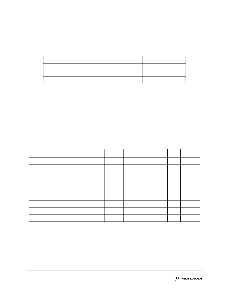
Electrical and Thermal Characteristics
The XPC750P incorporates a thermal management assist unit (TAU) composed of a thermal sensor, digital-
to-analog converter, comparator, control logic, and dedicated special-purpose registers (SPRs). See the
MPC750 RISC Microprocessor Users Manual for more information on the use of this feature.
Specications for the thermal sensor portion of the TAU are found in Table 5..
Table 6. provides the DC electrical characteristics for the XPC750P.
Table 5. Thermal Sensor Specifications
At recommended operating conditions (See Table 3.)
Characteristic
Min
Max
Unit
Notes
Temperature range
0
127
C
1
Comparator settling time
20
s
2
Resolution
4
C
3
Notes:
1. The temperature is the junction temperature of the die. The thermal assist units raw
output does not indicate an absolute temperature, but it must be interpreted by
software to derive the absolute junction temperature. For information about the use
and calibration of the TAU, see Motorola Application Note AN1800/D, Programming
the Thermal Assist Unit in the MPC750 Microprocessor.
2. The comparator settling time value must be converted into the number of CPU clocks
that need to be written into the THRM3 SPR.
3. Guaranteed by design and characterization.
Table 6. DC Electrical Specifications
At recommended operating conditions (See Table 3.)
Characteristic
Symbol
Min
Max
Unit
Notes
Input high voltage (all inputs except SYSCLK)
VIH
2
OVdd + 0.3
V
2,3
Input low voltage (all inputs except SYSCLK)
VIL
-0.3
0.8
V
SYSCLK input high voltage
CVIH
2.4
OVdd + 0.3
V
2
SYSCLK input low voltage
CVIL
-0.3
0.4
V
Input leakage current, Vin = OVdd
Iin
30
A
2,3
Hi-Z (off-state) leakage current, Vin = OVdd
ITSI
30
A
2,3,5
Output high voltage, IOH = -6 mA
VOH
2.4
V
Output low voltage, IOL = 6 mA
VOL
0.4
V
Capacitance, Vin = 0 V, f = 1 MHz
Cin
5.0
pF
3,4
Notes:
1. Nominal voltages; See Table 3. for recommended operating conditions.
2. For 60x bus signals, the reference is OVdd while L2OVdd is the reference for the L2 bus signals.
3. Excludes test signals (LSSD_MODE, L1_TSTCLK, L2_TSTCLK) and IEEE 1149.1 boundary scan (JTAG)
signals.
4. Capacitance is periodically sampled rather than 100% tested.
5. The leakage is measured for nominal OVdd and Vdd, or both OVdd and Vdd must vary in the same
direction (for example, both OVdd and Vdd vary by either +5% or -5%).
F
re
e
sc
a
le
S
e
m
ic
o
n
d
u
c
to
r,
I
Freescale Semiconductor, Inc.
For More Information On This Product,
Go to: www.freescale.com
n
c
..
.
相關(guān)PDF資料 |
PDF描述 |
|---|---|
| MPC740PRX333LE | 32-BIT, 333 MHz, RISC PROCESSOR, CBGA255 |
| MPC755BRX300LX | 32-BIT, 300 MHz, RISC PROCESSOR, CBGA360 |
| MPC745BPX400LX | 32-BIT, 400 MHz, RISC PROCESSOR, PBGA255 |
| MPC755BPX300LX | 32-BIT, 300 MHz, RISC PROCESSOR, PBGA360 |
| MPC755BRX400LX | 32-BIT, 400 MHz, RISC PROCESSOR, CBGA360 |
相關(guān)代理商/技術(shù)參數(shù) |
參數(shù)描述 |
|---|---|
| MPC7410 | 制造商:FREESCALE 制造商全稱:Freescale Semiconductor, Inc 功能描述:RISC Microprocessor Hardware Specifications Addendum |
| MPC7410_1 | 制造商:FREESCALE 制造商全稱:Freescale Semiconductor, Inc 功能描述:RISC Microprocessor Hardware Specifications |
| MPC7410_10 | 制造商:FREESCALE 制造商全稱:Freescale Semiconductor, Inc 功能描述:RISC Microprocessor Hardware Specifications Addendum |
| MPC74-103J | 制造商:未知廠家 制造商全稱:未知廠家 功能描述:Metal Plate Cement Resistors |
| MPC74-103K | 制造商:未知廠家 制造商全稱:未知廠家 功能描述:Metal Plate Cement Resistors |
發(fā)布緊急采購,3分鐘左右您將得到回復(fù)。