- 您現(xiàn)在的位置:買賣IC網(wǎng) > PDF目錄45365 > MPC8377EVRALGA (FREESCALE SEMICONDUCTOR INC) 32-BIT, 400 MHz, MICROPROCESSOR, PBGA689 PDF資料下載
參數(shù)資料
| 型號: | MPC8377EVRALGA |
| 廠商: | FREESCALE SEMICONDUCTOR INC |
| 元件分類: | 微控制器/微處理器 |
| 英文描述: | 32-BIT, 400 MHz, MICROPROCESSOR, PBGA689 |
| 封裝: | 31 X 31 MM, 2.46 MM HEIGHT, 1 MM PITCH, LEAD FREE, PLASTIC, BGA-689 |
| 文件頁數(shù): | 109/124頁 |
| 文件大小: | 1462K |
| 代理商: | MPC8377EVRALGA |
第1頁第2頁第3頁第4頁第5頁第6頁第7頁第8頁第9頁第10頁第11頁第12頁第13頁第14頁第15頁第16頁第17頁第18頁第19頁第20頁第21頁第22頁第23頁第24頁第25頁第26頁第27頁第28頁第29頁第30頁第31頁第32頁第33頁第34頁第35頁第36頁第37頁第38頁第39頁第40頁第41頁第42頁第43頁第44頁第45頁第46頁第47頁第48頁第49頁第50頁第51頁第52頁第53頁第54頁第55頁第56頁第57頁第58頁第59頁第60頁第61頁第62頁第63頁第64頁第65頁第66頁第67頁第68頁第69頁第70頁第71頁第72頁第73頁第74頁第75頁第76頁第77頁第78頁第79頁第80頁第81頁第82頁第83頁第84頁第85頁第86頁第87頁第88頁第89頁第90頁第91頁第92頁第93頁第94頁第95頁第96頁第97頁第98頁第99頁第100頁第101頁第102頁第103頁第104頁第105頁第106頁第107頁第108頁當(dāng)前第109頁第110頁第111頁第112頁第113頁第114頁第115頁第116頁第117頁第118頁第119頁第120頁第121頁第122頁第123頁第124頁
MPC8377E PowerQUICC II Pro Processor Hardware Specifications, Rev. 2
Freescale Semiconductor
85
High-Speed Serial Interfaces (HSSI)
occurs in the 1–15 MHz range. The source impedance of the clock driver should be 50
Ω to match the
transmission line and reduce reflections which are a source of noise to the system.
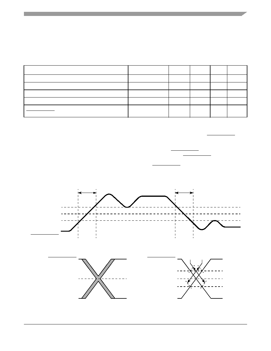
Table 70 describes some AC parameters common to PCI Express and SATA protocols.
Figure 60. Differential Measurement Points for Rise and Fall Time
Figure 61. Single-Ended Measurement Points for Rise and Fall Time Matching
Table 70. SerDes Reference Clock Common AC Parameters
At recommended operating conditions with XVDD_SRDS or XVDD_SRDS = 1.0 V ± 5%.
Parameter
Symbol
Min
Max
Unit
Notes
Rising Edge Rate
Rise Edge Rate
1.0
4.0
V/ns
Falling Edge Rate
Fall Edge Rate
1.0
4.0
V/ns
Differential Input High Voltage
VIH
200
—
mV
Differential Input Low Voltage
VIL
—
–200
mV
Rising edge rate (SD
n_REF_CLK) to falling edge rate
(SD
n_REF_CLK) matching
Rise-Fall Matching
—
20
%
Note:
1 Measurement taken from single ended waveform.
2 Measurement taken from differential waveform.
3 Measured from –200 mV to +200 mV on the differential waveform (derived from SDn_REF_CLK minus SDn_REF_CLK). The
signal must be monotonic through the measurement region for rise and fall time. The 400 mV measurement window is
centered on the differential zero crossing. See Figure 60.
4 Matching applies to rising edge rate for SDn_REF_CLK and falling edge rate for SDn_REF_CLK. It is measured using a
200 mV window centered on the median cross point where SDn_REF_CLK rising meets SD
n_REF_CLK falling. The median
cross point is used to calculate the voltage thresholds the oscilloscope is to use for the edge rate calculations. The Rise Edge
Rate of SD
n_REF_CLK should be compared to the Fall Edge Rate of SDn_REF_CLK, the maximum allowed difference
should not exceed 20% of the slowest edge rate. See Figure 61.
VIH = +200 mV
0.0 V
VIL = –200 mV
SD
n_REF_CLK
Minus
SD
n_REF_CLK
Rise Edge Rate
Fall Edge Rate
TFALL TRISE
SD
n_REF_CLK
VCROSS MEDIAN
SD
n_REF_CLK
SD
n_REF_CLK
VCROSS MEDIAN
SD
n_REF_CLK
VCROSS MEDIAN –100 mV
VCROSS MEDIAN +100 mV
相關(guān)PDF資料 |
PDF描述 |
|---|---|
| MPC8377EVRANGA | 32-BIT, 400 MHz, MICROPROCESSOR, PBGA689 |
| MPC8378ECVRALGA | 32-BIT, 400 MHz, MICROPROCESSOR, PBGA689 |
| MPC8378ECVRAGFA | 32-BIT, 333 MHz, MICROPROCESSOR, PBGA689 |
| MPC8378ECVRAGGA | 32-BIT, 400 MHz, MICROPROCESSOR, PBGA689 |
| MPC8378ECVRALFA | 32-BIT, 333 MHz, MICROPROCESSOR, PBGA689 |
相關(guān)代理商/技術(shù)參數(shù) |
參數(shù)描述 |
|---|---|
| MPC8377EVRANDA | 制造商:FREESCALE 制造商全稱:Freescale Semiconductor, Inc 功能描述:PowerQUICC? II Pro Processor Hardware Specifications |
| MPC8377EVRANFA | 制造商:FREESCALE 制造商全稱:Freescale Semiconductor, Inc 功能描述:PowerQUICC? II Pro Processor Hardware Specifications |
| MPC8377EVRANG | 功能描述:微處理器 - MPU 837X Encyrpted RoHS:否 制造商:Atmel 處理器系列:SAMA5D31 核心:ARM Cortex A5 數(shù)據(jù)總線寬度:32 bit 最大時鐘頻率:536 MHz 程序存儲器大小:32 KB 數(shù)據(jù) RAM 大小:128 KB 接口類型:CAN, Ethernet, LIN, SPI,TWI, UART, USB 工作電源電壓:1.8 V to 3.3 V 最大工作溫度:+ 85 C 安裝風(fēng)格:SMD/SMT 封裝 / 箱體:FBGA-324 |
| MPC8377EVRANGA | 功能描述:微處理器 - MPU 8377 PBGA ST PbFr W/ENC RoHS:否 制造商:Atmel 處理器系列:SAMA5D31 核心:ARM Cortex A5 數(shù)據(jù)總線寬度:32 bit 最大時鐘頻率:536 MHz 程序存儲器大小:32 KB 數(shù)據(jù) RAM 大小:128 KB 接口類型:CAN, Ethernet, LIN, SPI,TWI, UART, USB 工作電源電壓:1.8 V to 3.3 V 最大工作溫度:+ 85 C 安裝風(fēng)格:SMD/SMT 封裝 / 箱體:FBGA-324 |
| MPC8377EWLANA | 功能描述:開發(fā)板和工具包 - 其他處理器 MPC8377EWLANA, KIT RoHS:否 制造商:Freescale Semiconductor 產(chǎn)品:Development Systems 工具用于評估:P3041 核心:e500mc 接口類型:I2C, SPI, USB 工作電源電壓: |
發(fā)布緊急采購,3分鐘左右您將得到回復(fù)。