- 您現(xiàn)在的位置:買賣IC網(wǎng) > PDF目錄17039 > MPC8536E-ANDROID (Freescale Semiconductor)HARDWARE/SOFTWARE ANDROID OS PDF資料下載
參數(shù)資料
| 型號: | MPC8536E-ANDROID |
| 廠商: | Freescale Semiconductor |
| 文件頁數(shù): | 11/126頁 |
| 文件大小: | 0K |
| 描述: | HARDWARE/SOFTWARE ANDROID OS |
| 標(biāo)準(zhǔn)包裝: | 1 |
| 系列: | PowerQUICC ™ |
| 類型: | MPU |
| 適用于相關(guān)產(chǎn)品: | MPC8536 |
| 所含物品: | 板 |
第1頁第2頁第3頁第4頁第5頁第6頁第7頁第8頁第9頁第10頁當(dāng)前第11頁第12頁第13頁第14頁第15頁第16頁第17頁第18頁第19頁第20頁第21頁第22頁第23頁第24頁第25頁第26頁第27頁第28頁第29頁第30頁第31頁第32頁第33頁第34頁第35頁第36頁第37頁第38頁第39頁第40頁第41頁第42頁第43頁第44頁第45頁第46頁第47頁第48頁第49頁第50頁第51頁第52頁第53頁第54頁第55頁第56頁第57頁第58頁第59頁第60頁第61頁第62頁第63頁第64頁第65頁第66頁第67頁第68頁第69頁第70頁第71頁第72頁第73頁第74頁第75頁第76頁第77頁第78頁第79頁第80頁第81頁第82頁第83頁第84頁第85頁第86頁第87頁第88頁第89頁第90頁第91頁第92頁第93頁第94頁第95頁第96頁第97頁第98頁第99頁第100頁第101頁第102頁第103頁第104頁第105頁第106頁第107頁第108頁第109頁第110頁第111頁第112頁第113頁第114頁第115頁第116頁第117頁第118頁第119頁第120頁第121頁第122頁第123頁第124頁第125頁第126頁
MPC8536E PowerQUICC III Integrated Processor Hardware Specifications, Rev. 5
Electrical Characteristics
Freescale Semiconductor
108
2.23.2
CCB/SYSCLK PLL Ratio
The CCB clock is the clock that drives the e500 core complex bus (CCB), and is also called the platform clock. The frequency
of the CCB is set using the following reset signals, as shown in the following table:
SYSCLK input signal
Binary value on LA[28:31] at power up
Note that there is no default for this PLL ratio; these signals must be pulled to the desired values.
2.23.3
e500 Core PLL Ratio
This table describes the clock ratio between the e500 core complex bus (CCB) and the e500 core clock. This ratio is determined
by the binary value of LBCTL, LALE and LGPL2 at power up, as shown in this table.
2.23.4
DDR/DDRCLK PLL Ratio
The DDR memory controller complex can be synchronous with, or asynchronous to, the CCB, depending on configuration.
The following table describes the clock ratio between the DDR memory controller complex and the DDR/DDRCLK PLL
reference clock, DDRCLK, which is not the memory bus clock.
When synchronous mode is selected, the memory buses are clocked at half the CCB clock rate. The default mode of operation
is for the DDR data rate for the DDR controller to be equal to the CCB clock rate in synchronous mode, or the resulting DDR
PLL rate in asynchronous mode.
In asynchronous mode, the DDR PLL rate to DDRCLK ratios listed in Table 77 reflects the DDR data rate to DDRCLK ratio,
since the DDR PLL rate in asynchronous mode means the DDR data rate resulting from DDR PLL output.
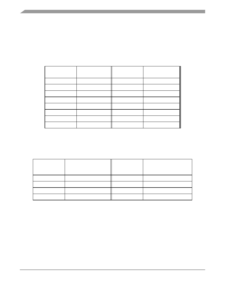
Table 75. CCB Clock Ratio
Binary Value of
LA[28:31] Signals
CCB:SYSCLK Ratio
Binary Value of
LA[28:31] Signals
CCB:SYSCLK Ratio
0000
16:1
1000
8:1
0001
Reserved
1001
9:1
0010
Reserved
1010
10:1
0011
3:1
1011
Reserved
0100
4:1
1100
12:1
0101
5:1
1101
Reserved
0110
6:1
1110
Reserved
0111
Reserved
1111
Reserved
Table 76. e500 Core to CCB Clock Ratio
Binary Value of
LBCTL, LALE,
LGPL2 Signals
e500 core: CCB Clock Ratio
Binary Value of
LBCTL, LALE,
LGPL2 Signals
e500 core: CCB Clock Ratio
000
4:1
100
2:1
001
9:2
101
5:2
010
Reserved
110
3:1
011
3:2
111
7:2
相關(guān)PDF資料 |
PDF描述 |
|---|---|
| 0210490966 | CABLE JUMPER 1.25MM .051M 27POS |
| 0210391099 | CABLE JUMPER 1MM .051M 39POS |
| EVAL-AD7666CBZ | BOARD EVALUATION FOR AD7666 |
| MLK1005S5N1S | INDUCTOR MULTILAYER 5.1NH 0402 |
| 0210490323 | CABLE JUMPER 1.25MM .051M 26POS |
相關(guān)代理商/技術(shù)參數(shù) |
參數(shù)描述 |
|---|---|
| MPC8536EAVTAKG | 功能描述:微處理器 - MPU PQ38S 8536 SQUID RoHS:否 制造商:Atmel 處理器系列:SAMA5D31 核心:ARM Cortex A5 數(shù)據(jù)總線寬度:32 bit 最大時鐘頻率:536 MHz 程序存儲器大小:32 KB 數(shù)據(jù) RAM 大小:128 KB 接口類型:CAN, Ethernet, LIN, SPI,TWI, UART, USB 工作電源電壓:1.8 V to 3.3 V 最大工作溫度:+ 85 C 安裝風(fēng)格:SMD/SMT 封裝 / 箱體:FBGA-324 |
| MPC8536EAVTAKGA | 功能描述:微處理器 - MPU 8536 Encrypted RoHS:否 制造商:Atmel 處理器系列:SAMA5D31 核心:ARM Cortex A5 數(shù)據(jù)總線寬度:32 bit 最大時鐘頻率:536 MHz 程序存儲器大小:32 KB 數(shù)據(jù) RAM 大小:128 KB 接口類型:CAN, Ethernet, LIN, SPI,TWI, UART, USB 工作電源電壓:1.8 V to 3.3 V 最大工作溫度:+ 85 C 安裝風(fēng)格:SMD/SMT 封裝 / 箱體:FBGA-324 |
| MPC8536EAVTANG | 功能描述:微處理器 - MPU PQ38S 8536 SQUID RoHS:否 制造商:Atmel 處理器系列:SAMA5D31 核心:ARM Cortex A5 數(shù)據(jù)總線寬度:32 bit 最大時鐘頻率:536 MHz 程序存儲器大小:32 KB 數(shù)據(jù) RAM 大小:128 KB 接口類型:CAN, Ethernet, LIN, SPI,TWI, UART, USB 工作電源電壓:1.8 V to 3.3 V 最大工作溫度:+ 85 C 安裝風(fēng)格:SMD/SMT 封裝 / 箱體:FBGA-324 |
| MPC8536EAVTANGA | 功能描述:微處理器 - MPU 8536 Encrypted RoHS:否 制造商:Atmel 處理器系列:SAMA5D31 核心:ARM Cortex A5 數(shù)據(jù)總線寬度:32 bit 最大時鐘頻率:536 MHz 程序存儲器大小:32 KB 數(shù)據(jù) RAM 大小:128 KB 接口類型:CAN, Ethernet, LIN, SPI,TWI, UART, USB 工作電源電壓:1.8 V to 3.3 V 最大工作溫度:+ 85 C 安裝風(fēng)格:SMD/SMT 封裝 / 箱體:FBGA-324 |
| MPC8536EAVTAQG | 功能描述:微處理器 - MPU PQ38S 8536 SQUID RoHS:否 制造商:Atmel 處理器系列:SAMA5D31 核心:ARM Cortex A5 數(shù)據(jù)總線寬度:32 bit 最大時鐘頻率:536 MHz 程序存儲器大小:32 KB 數(shù)據(jù) RAM 大小:128 KB 接口類型:CAN, Ethernet, LIN, SPI,TWI, UART, USB 工作電源電壓:1.8 V to 3.3 V 最大工作溫度:+ 85 C 安裝風(fēng)格:SMD/SMT 封裝 / 箱體:FBGA-324 |
發(fā)布緊急采購,3分鐘左右您將得到回復(fù)。