- 您現(xiàn)在的位置:買賣IC網(wǎng) > PDF目錄69037 > MPC972FA (FREESCALE SEMICONDUCTOR INC) 125 MHz, PROC SPECIFIC CLOCK GENERATOR, PQFP52 PDF資料下載
參數(shù)資料
| 型號: | MPC972FA |
| 廠商: | FREESCALE SEMICONDUCTOR INC |
| 元件分類: | 時鐘產(chǎn)生/分配 |
| 英文描述: | 125 MHz, PROC SPECIFIC CLOCK GENERATOR, PQFP52 |
| 封裝: | LQFP-52 |
| 文件頁數(shù): | 3/12頁 |
| 文件大小: | 337K |
| 代理商: | MPC972FA |
MPC972
MOTOROLA ADVANCED CLOCK DRIVERS DEVICE DATA
196
MPC972. From the data sheet the IVCCA current (the current
sourced through the VCCA pin) is typically 15 mA (20 mA
maximum), assuming that a minimum of 2.935 V must be
maintained on the VCCA pin very little DC voltage drop can be
tolerated when a 3.3 V VCC supply is used. The resistor shown
in Figure 11 must have a resistance of 5–10
to meet the
voltage drop criteria. The RC filter pictured will provide a
broadband filter with approximately 100:1 attenuation for noise
whose spectral content is above 20 KHz. As the noise
frequency crosses the series resonant point of an individual
capacitor it’s overall impedance begins to look inductive and
thus increases with increasing frequency. The parallel capacitor
combination shown ensures that a low impedance path to
ground exists for frequencies well above the bandwidth of the
PLL.
Although the MPC972 has several design features to
minimize the susceptibility to power supply noise (isolated
power and grounds and fully differential PLL) there still may be
applications in which overall performance is being degraded
due to system power supply noise. The power supply filter
schemes discussed in this section should be adequate to
eliminate power supply noise related problems in most designs.
Driving Transmission Lines
The MPC972 clock driver was designed to drive high speed
signals in a terminated transmission line environment. To
provide the optimum flexibility to the user the output drivers
were designed to exhibit the lowest impedance possible. With
an output impedance of approximately 10
the drivers can
drive either parallel or series terminated transmission lines. For
more information on transmission lines the reader is referred to
application note AN1091 in the Timing Solutions data book
(DL207/D).
In most high performance clock networks point–to–point
distribution of signals is the method of choice. In a point–to–
point scheme either series terminated or parallel terminated
transmission lines can be used. The parallel technique termi-
nates the signal at the end of the line with a
50
resistance to VCC/2. This technique draws a fairly high
level of DC current and thus only a single terminated line can be
driven by each output of the MPC972 clock driver. For the series
terminated case however there is no DC current draw, thus the
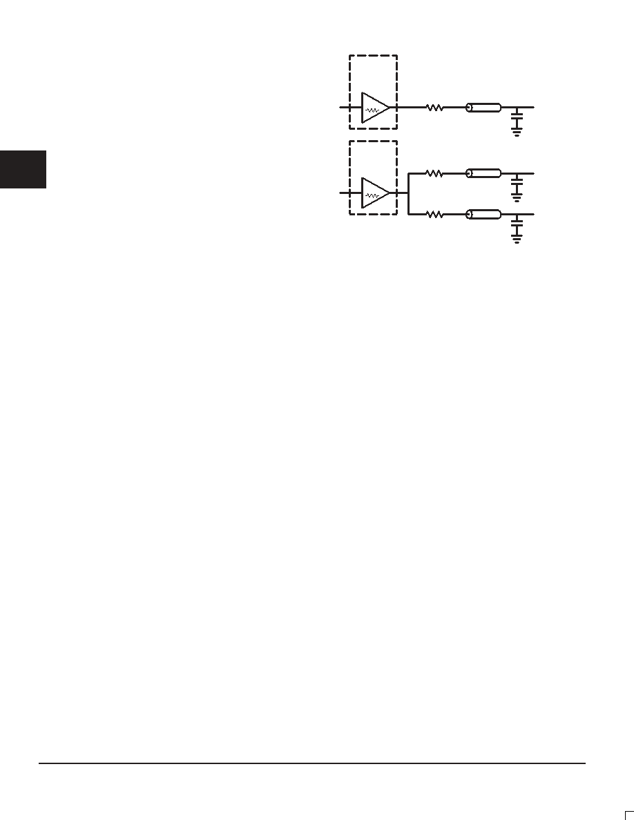
outputs can drive multiple series terminated lines. Figure 12
illustrates an output driving a single series terminated line vs
two series terminated lines in parallel. When taken to its
extreme the fanout of the MPC972 clock driver is effectively
doubled due to its capability to drive multiple lines.
Figure 12. Single versus Dual Transmission Lines
7
IN
MPC972
OUTPUT
BUFFER
RS = 43
ZO = 50
OutA
7
IN
MPC972
OUTPUT
BUFFER
RS = 43
ZO = 50
OutB0
RS = 43
ZO = 50
OutB1
The waveform plots of Figure 13 show the simulation results
of an output driving a single line vs two lines. In both cases the
drive capability of the MPC972 output buffers is more than
sufficient to drive 50
transmission lines on the incident edge.
Note from the delay measurements in the simulations a delta of
only 43 ps exists between the two differently loaded outputs.
This suggests that the dual line driving need not be used
exclusively to maintain the tight output–to–output skew of the
MPC972. The output waveform in Figure 13 shows a step in the
waveform, this step is caused by the impedance mismatch seen
looking into the driver. The parallel combination of the
43
series resistor plus the output impedance does not match
the parallel combination of the line impedances. The voltage
wave launched down the two lines will equal:
VL = VS ( Zo / Rs + Ro +Zo) = 3.0 (25/53.5) = 1.40 V
At the load end the voltage will double, due to the near unity
reflection coefficient, to 2.8 V. It will then increment towards the
quiescent 3.0 V in steps separated by one round trip delay (in
this case 4.0 ns).
Since this step is well above the threshold region it will not
cause any false clock triggering, however designers may be
uncomfortable with unwanted reflections on the line. To better
match the impedances when driving multiple lines the situation
in Figure 14 should be used. In this case the series terminating
resistors are reduced such that when the parallel combination
is added to the output buffer impedance the line impedance is
perfectly matched.
2
F
re
e
sc
a
le
S
e
m
ic
o
n
d
u
c
to
r,
I
Freescale Semiconductor, Inc.
For More Information On This Product,
Go to: www.freescale.com
n
c
..
.
相關(guān)PDF資料 |
PDF描述 |
|---|---|
| MPC9850VF | 500 MHz, PROC SPECIFIC CLOCK GENERATOR, PBGA100 |
| MPC9850VMR2 | 500 MHz, PROC SPECIFIC CLOCK GENERATOR, PBGA100 |
| MPC9850VMR2 | 500 MHz, PROC SPECIFIC CLOCK GENERATOR, PBGA100 |
| MPC9850VFR2 | 500 MHz, PROC SPECIFIC CLOCK GENERATOR, PBGA100 |
| MPC9992FAR2 | 400 MHz, OTHER CLOCK GENERATOR, PQFP32 |
相關(guān)代理商/技術(shù)參數(shù) |
參數(shù)描述 |
|---|---|
| MPC972H10 F44A WAF | 制造商:Motorola Inc 功能描述: |
| MPC973 | 制造商:MOTOROLA 制造商全稱:Motorola, Inc 功能描述:LOW VOLTAGE PLL CLOCK DRIVER |
| MPC974 | 制造商:MOTOROLA 制造商全稱:Motorola, Inc 功能描述:LOW VOLTAGE PLL CLOCK DRIVER |
| MPC974A44 F44A WAF | 制造商:Motorola Inc 功能描述: |
| MPC9772 | 制造商:MOTOROLA 制造商全稱:Motorola, Inc 功能描述:3.3V 1:12 LVCMOS PLL Clock Generator |
發(fā)布緊急采購,3分鐘左右您將得到回復(fù)。