- 您現(xiàn)在的位置:買賣IC網(wǎng) > PDF目錄296638 > MSK5930KRHS (MS KENNEDY CORP) DUAL OUTPUT, FIXED MIXED LDO REGULATOR, SFM5 PDF資料下載
參數(shù)資料
| 型號(hào): | MSK5930KRHS |
| 廠商: | MS KENNEDY CORP |
| 元件分類: | 固定混合多路輸出LDO穩(wěn)壓器 |
| 英文描述: | DUAL OUTPUT, FIXED MIXED LDO REGULATOR, SFM5 |
| 封裝: | STRAIGHT, SIP-5 |
| 文件頁(yè)數(shù): | 2/5頁(yè) |
| 文件大小: | 192K |
| 代理商: | MSK5930KRHS |
1
2
3
4
5
6
7
8
9
10
11
2
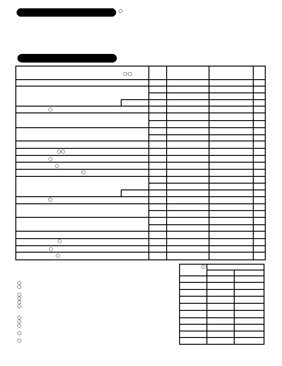
POSITIVE OUTPUT REGULATORS
Dropout Voltage
Quiescent Current
Short Circuit Current
Ripple Rejection
Thermal Resistance
NEGATIVE OUTPUT REGULATORS
Dropout Voltage
Quiescent Current
Short Circuit Current
Ripple Rejection
Thermal Resistance
0A
≤IOUT≤3A; VOUT=50mV
100mA
≤IOUT≤3A
VIN=VOUT+3V
IOUT=0A
(VOUT+3V)
≤VIN≤(VOUT+15V)
VIN=VOUT+3V; IOUT=0A
VIN=VOUT+5V
IOUT=3A; COUT=25F; f=120Hz
JUNCTION TO CASE @ 125°C
0A
≤IOUT≤3A; VOUT=50mV
VIN=VOUT+3V
100mA
≤IOUT≤3A
IOUT=0A
(VOUT+3V)
≤VIN≤(VOUT+15V)
VIN=VOUT+3V; IOUT=0A
VIN=VOUT+5V
IOUT=3A; COUT=25F; f=120Hz
JUNCTION TO CASE @ 125°C
Max.
1.0
2.0
3.0
1.5
1
2
0.5
0.75
15
-
3.2
1.0
2.5
2.0
1.2
1
2
0.5
0.75
10
-
3.6
Storage Temperature Range
Lead Temperature Range
(10 Seconds)
Case Operating Temperature
MSK 5930-5939RH
MSK 5930K/H/E RH-
5939K/H/E RH
±30V
Internally Limited
±3A
+150°C
-65°C to +150°C
300°C
-40°C to +85°C
-55°C to +125°C
ABSOLUTE MAXIMUM RATINGS
TST
TLD
TC
Input Voltage (WRT VOUT)
Power Dissipation
Output Current
Junction Temperature
○
○○○○○
○
○○○○○○○○
±VIN
PD
IOUT
TJ
○○○○
○
○○○○○○○○○○○○○
○
○○○○○○○
○○○○
○
○○○○○
Outputs are decoupled to ground using 33F minimum low ESR capacitors unless otherwise specified.
Guaranteed by design but not tested. Typical parameters are representative of actual device
performance but are for reference only.
All output parameters are tested using a low duty cycle pulse to maintain TJ = TC.
Industrial grade and "E" suffix devices shall be tested to subgroup 1 unless otherwise specified.
Military grade devices ("H" and "K" suffix) shall be 100% tested to subgroups 1,2 and 3.
Subgroup 1
TA=TC=+25°C
Subgroup 2
TA=TC=+125°C
Subgroup 3
TA=TC=-55°C
Please consult the factory if alternate output voltages are required.
Input voltage (VIN= VOUT + a specified voltage) is implied to be more negative than VOUT.
For compliance with Mil-STD 833 revision C current density specifications, the MSK 5930RH series is
derated to 2 Amps for the positive regulator.
Continuous operation at or above absolute maximum ratings may adversely effect the device
performance and/or life cycle.
Pre and post irradiation limits, at 25°C, up to 100Krad TID, are identical unless otherwise specified.
Min.
-
3.0
60
-
3.0
60
-
Group A
Subgroup
1
2,3
1
2,3
1
2,3
1,2,3
-
1
2,3
1
2,3
1
2,3
1,2,3
-
Min.
-
3.2
60
-
3.0
60
-
Typ.
0.1
1.5
1.3
0.2
0.3
0.1
0.2
10
4
75
2.9
0.1
1.0
0.8
0.2
0.3
0.1
0.2
4.5
3.5
75
3.3
Typ.
0.1
-
1.5
1.3
0.2
-
0.1
-
10
4
75
2.9
0.1
-
1.0
0.8
0.2
-
0.1
-
4.5
3.5
75
3.3
Max.
2.0
-
3.0
1.6
2
-
0.6
-
15
-
3.2
2.0
-
2.0
1.3
2
-
0.6
-
10
-
3.6
Parameter
ELECTRICAL SPECIFICATIONS
Test Conditions
Units
MSK 5930RH SERIES
MSK 5930K/H/E RH
SERIES
3
2
%
V
%
mA
A
dB
°C/W
%
V
%
mA
A
dB
°C/W
8
2
NOTES:
2
9
Rev. C 12/08
11
Post Radiation
Output Voltage Tolerance
IOUT=0A; VIN=VOUT+3V
Load Regulation
Line Regulation
Post Radiation
Output Voltage Tolerance
IOUT=0A; VIN=VOUT+3V
Load Regulation
Line Regulation
+3.3V
+5.0V
+12.0V
+15.0V
+5.0V
+10.0V
MSK5930RH
MSK5931RH
MSK5932RH
MSK5933RH
MSK5934RH
MSK5935RH
MSK5936RH
MSK5937RH
MSK5938RH
MSK5939RH
-5.2V
-5.0V
-5.2V
-5.0V
-12.0V
-15.0V
-5.0V
-12.0V
-15.0V
-10.0V
OUTPUT VOLTAGES
POSITIVE
NEGATIVE
7
9
PART
NUMBER
相關(guān)PDF資料 |
PDF描述 |
|---|---|
| MSK5930KRHU | DUAL OUTPUT, FIXED MIXED LDO REGULATOR, SFM5 |
| MSK5940-5.0ERHG | 5 V FIXED NEGATIVE LDO REGULATOR, 1 V DROPOUT, PSSO3 |
| MSK5940-5.0ERHTD | 5 V FIXED NEGATIVE LDO REGULATOR, 1 V DROPOUT, SFM3 |
| MSK5940-5.0ERHTS | 5 V FIXED NEGATIVE LDO REGULATOR, 1 V DROPOUT, SFM3 |
| MSK5940-5.0HRHG | 5 V FIXED NEGATIVE LDO REGULATOR, 1 V DROPOUT, PSSO3 |
相關(guān)代理商/技術(shù)參數(shù) |
參數(shù)描述 |
|---|---|
| MSK600 | 制造商:MSK 制造商全稱:M.S. Kennedy Corporation 功能描述:WIDE BANDWIDTH HIGH VOLTAGE AMPLIFIER |
| MSK601 | 制造商:MSK 制造商全稱:M.S. Kennedy Corporation 功能描述:WIDE BANDWIDTH HIGH VOLTAGE AMPLIFIER |
| MSK601B | 制造商:MSK 制造商全稱:M.S. Kennedy Corporation 功能描述:WIDE BANDWIDTH HIGH VOLTAGE AMPLIFIER |
| MSK604 | 制造商:MSK 制造商全稱:M.S. Kennedy Corporation 功能描述:NEGATIVE OUTPUT WIDE BANDWIDTH HIGH VOLTAGE AMPLIFIER |
| MSK604B | 制造商:MSK 制造商全稱:M.S. Kennedy Corporation 功能描述:NEGATIVE OUTPUT WIDE BANDWIDTH HIGH VOLTAGE AMPLIFIER |
發(fā)布緊急采購(gòu),3分鐘左右您將得到回復(fù)。