- 您現(xiàn)在的位置:買(mǎi)賣(mài)IC網(wǎng) > PDF目錄378017 > MSM7583 (OKI SEMICONDUCTOR CO., LTD.) pie/4 Shift QPSK MODEM PDF資料下載
參數(shù)資料
| 型號(hào): | MSM7583 |
| 廠商: | OKI SEMICONDUCTOR CO., LTD. |
| 英文描述: | pie/4 Shift QPSK MODEM |
| 中文描述: | 餡餅/ 4移調(diào)制調(diào)制解調(diào)器 |
| 文件頁(yè)數(shù): | 9/23頁(yè) |
| 文件大小: | 215K |
| 代理商: | MSM7583 |
第1頁(yè)第2頁(yè)第3頁(yè)第4頁(yè)第5頁(yè)第6頁(yè)第7頁(yè)第8頁(yè)當(dāng)前第9頁(yè)第10頁(yè)第11頁(yè)第12頁(yè)第13頁(yè)第14頁(yè)第15頁(yè)第16頁(yè)第17頁(yè)第18頁(yè)第19頁(yè)第20頁(yè)第21頁(yè)第22頁(yè)第23頁(yè)
9/23
MSM7583
Semiconductor
RXSEL
Receive data, receive clock, and receive symbol clock select signal.
If this pin is set to "0", the output levels of Channel 1 RXD1, RXC1, and RXSC1 are selected to
be output to RXD0, RXC0, and RXSC0. If this pin is set to "1", the output levels of Channel 2
RXD2, RXC2, and RXSC2 are selected to be output to RXD0, RXC0, and RXSC0.
Note that a hazard may sometime occur in RXDO, RXCO, and RXSCO because RXSEL selects
asynchronously.
RPR1, RPR2
High-speed phase clock control signal input pin for the clock recovery circuit.
When each of the pins is “1”, the clock recovery circuit starts in the high-speed phase clock
mode. When the phase difference is less than a defined value, the circuit shifts to the low-speed
phase clock mode automatically. When each of the pins is “0”, the circuit is always in the low-
speed phase clock mode. RPR1 is for Channel 1, and RPR2 for Channel 2.
AFC1, AFC2
AFC operation range specification signal inputs.
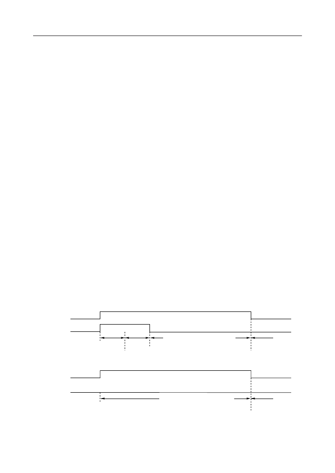
As shown in Fig. 4, the AFC information is reset when both AFC and RPR are set to “1”. AFC
operation starts at a certain period after the AFC information is reset. When RPR is set to “1”,
an average number of times that AFC sets to on is low. When RPR is “0”, it is high. When AFC
is “0”, frequency error is not calculated, but the frequency is corrected using an error that is
held. AFC1 is for Channel 1, and AFC2 for Channel 2.
RCW1, RCW2
Clock recovery circuit operation ON/OFF control signal inputs.
When this pin is “0”, DPLL does not make any phase corrections. RCW1 is for Channel 1, and
RCW2 for Channel 2.
Figure 4 AFC Control Timing Diagram
AFC
RPR
(CASE1)
AFC information
is maintained.
AFC information
is reset.
Average
number of times
AFC is low.
Average number of times
AFC is high.
AFC
RPR
(CASE2)
AFC information
is maintained.
“0”
The clock recovery
circuit starts with the previous
AFC information.
Average number of times
AFC is high.
相關(guān)PDF資料 |
PDF描述 |
|---|---|
| MSM7584C | π/4 Shift QPSK MODEM(π/4移動(dòng)QPSK調(diào)制解調(diào)器/ADPCM編碼譯碼器) |
| MSM7590L-01 | Multi-Function ADPCM CODEC |
| MSM7590 | 5V Sinlge-Rail ADPCM CODECs |
| MSM7602 | Echo Canceler |
| MSM7602-001 | Echo Canceler |
相關(guān)代理商/技術(shù)參數(shù) |
參數(shù)描述 |
|---|---|
| MSM7583GS-BK | 制造商:OKI 制造商全稱(chēng):OKI electronic componets 功能描述:pie/4 Shift QPSK MODEM |
| MSM7584C | 制造商:OKI 制造商全稱(chēng):OKI electronic componets 功能描述:pi /4 Shift QPSK MODEM/ADPCM CODEC |
| MSM7584CTS-K | 制造商:OKI 制造商全稱(chēng):OKI electronic componets 功能描述:pi /4 Shift QPSK MODEM/ADPCM CODEC |
| MSM7584D | 制造商:OKI 制造商全稱(chēng):OKI electronic componets 功能描述:pi/4 Shift QPSK MODEM/ADPCM CODEC |
| MSM7584DTS-K | 制造商:OKI 制造商全稱(chēng):OKI electronic componets 功能描述:pi/4 Shift QPSK MODEM/ADPCM CODEC |
發(fā)布緊急采購(gòu),3分鐘左右您將得到回復(fù)。