- 您現(xiàn)在的位置:買賣IC網(wǎng) > PDF目錄378017 > MSM7602-011 (OKI SEMICONDUCTOR CO., LTD.) Echo Canceler PDF資料下載
參數(shù)資料
| 型號: | MSM7602-011 |
| 廠商: | OKI SEMICONDUCTOR CO., LTD. |
| 英文描述: | Echo Canceler |
| 中文描述: | 回聲消除器 |
| 文件頁數(shù): | 7/29頁 |
| 文件大?。?/td> | 238K |
| 代理商: | MSM7602-011 |
第1頁第2頁第3頁第4頁第5頁第6頁當前第7頁第8頁第9頁第10頁第11頁第12頁第13頁第14頁第15頁第16頁第17頁第18頁第19頁第20頁第21頁第22頁第23頁第24頁第25頁第26頁第27頁第28頁第29頁
Semiconductor
MSM7602
7/29
(3/5)
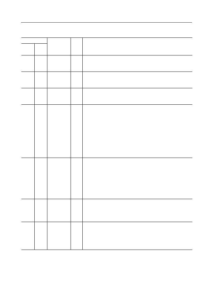
Pin
28-pin
SSOP
11
56-pin
QFP
11
Symbol
Type
Description
—
PD5
PD6
—
SYNC
I
12
12
SOUT
O
13
13
ROUT
O
—
—
—
—
—
—
—
—
15
—
20
22
—
27
29
30
44
45
PD0
PD11
PD12
PD13
PD14
PD15
I/O
17
31
X1/CLKIN
I
18
32
X2
O
16
28
HD
I
Sync signal for transmit/receive serial data.
This pin uses the external SYNC or SYNCO.
Input the PCM CODEC transmit/receive sync signal (8 kHz).
Transmit serial data.
Outputs the PCM signal synchronized to SYNC and SCK.
This pin is in a high impedance state during no data output.
Receive serial data.
Outputs the PCM signal synchronized to SYNC and SCK.
This pin is in a high impedance state during no data output.
This is the bidirectional bus pin for parallel data transfer between the
master chip and slave chip when used in a cascade connection.
The PD15 pin corresponds to MSB.
This pin is in a high impedance state during no data
output. Data is loaded in at the falling edge of
SFx
.
Controls the howling detect function.
This pin detets and cancels a howling
generated during hand-free talking for acoustic system.
This function is used to cancel acoustic echoes.
Single Chip or Master Chip in a Cascade Connection
"L": Howling detector ON
"H": Howling detector OFF
Slave Chip in a Cascade Connection
Fixed at "L"
External input for the basic clock (17.5 to 20 MHz) or for the crystal
oscillator.
When the internal sync signal (SYNCO, SCKO) is used, input the basic
clock of 19.2 MHz.
Crystal oscillator output.
Used to configure the oscilation circuit.
Refer to the internal clock generator circuit example.
When inputting the basic clock externally, insert a 5 pF capacitor with
excellent high frequency characteristics between X2 and GND.
相關(guān)PDF資料 |
PDF描述 |
|---|---|
| MSM7603 | Echo Canceler |
| MSM7603B | Echo Canceler |
| MSM7630 | Universal Speech Processor(通用語音處理器) |
| MSM7661B | NTSC/PAL Digital Dencoder(NTSC/PAL制式數(shù)字譯碼器) |
| MSM7661 | NTSC/PAL Digital Dencoder(NTSC/PAL制式數(shù)字譯碼器) |
相關(guān)代理商/技術(shù)參數(shù) |
參數(shù)描述 |
|---|---|
| MSM7603 | 制造商:OKI 制造商全稱:OKI electronic componets 功能描述:Echo Canceler |
| MSM7603B | 制造商:OKI 制造商全稱:OKI electronic componets 功能描述:Echo Canceler |
| MSM7617 | 制造商:OKI 制造商全稱:OKI electronic componets 功能描述:2-Channel Echo Canceler |
| MSM7620 | 制造商:OKI 制造商全稱:OKI electronic componets 功能描述:Echo Canceler |
| MSM7620-001GS-K | 制造商:OKI 制造商全稱:OKI electronic componets 功能描述:Echo Canceler |
發(fā)布緊急采購,3分鐘左右您將得到回復(fù)。