- 您現(xiàn)在的位置:買賣IC網(wǎng) > PDF目錄378018 > MSM7715 (OKI SEMICONDUCTOR CO., LTD.) Multi-Function Telecommunication LSI PDF資料下載
參數(shù)資料
| 型號(hào): | MSM7715 |
| 廠商: | OKI SEMICONDUCTOR CO., LTD. |
| 英文描述: | Multi-Function Telecommunication LSI |
| 中文描述: | 多功能通信大規(guī)模集成電路 |
| 文件頁(yè)數(shù): | 4/21頁(yè) |
| 文件大小: | 150K |
| 代理商: | MSM7715 |
第1頁(yè)第2頁(yè)第3頁(yè)當(dāng)前第4頁(yè)第5頁(yè)第6頁(yè)第7頁(yè)第8頁(yè)第9頁(yè)第10頁(yè)第11頁(yè)第12頁(yè)第13頁(yè)第14頁(yè)第15頁(yè)第16頁(yè)第17頁(yè)第18頁(yè)第19頁(yè)第20頁(yè)第21頁(yè)
Semiconductor
MSM7715
4/21
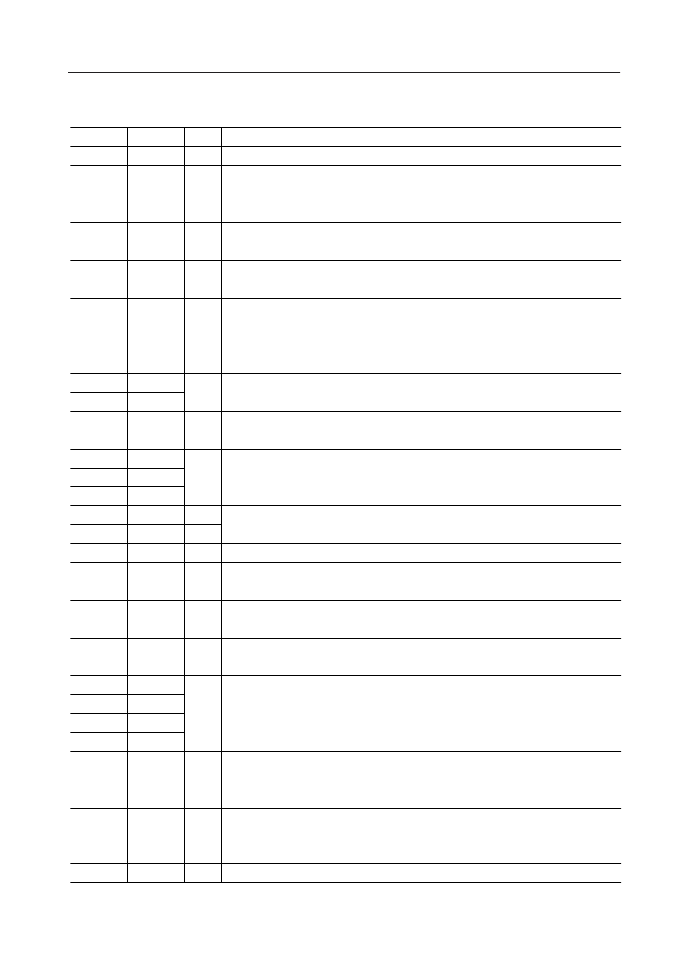
PIN DESCRIPTION
DTG4
Pin No.
1
I/O
I*
Name
TEN
2
TD
3
RS
4
CPW
5
ICTA
ICTB
6
7
DTTIM
8
MODE1
MODE2
MODE3
X1
X2
CLK
9
10
11
12
13
15
RD
16
CD
17
CP
18
DT1
DT2
DT3
DT4
19
20
21
22
SP
23
PON
24
AOUT
27
I*
I*
I*
I*
I*
I*
I*
I
O
O
O
O
O
O
O
I*
O
Description
Input for specifying the DTMF code to be sent.
Input for selecting the operation mode. See Table 1.
Outputs for the code of the received DTMF signal. In a mode other than the
DTMF receiving mode, these pins are in a high-impedance state.
Inputs for testing. Leave them open or connect them to V
DD
.
Input for controlling output of the DTMF signal. (Transmit enable)
DTG1 to DTG4 are latched at the falling edge of
TEN
and the DTMF signal is
output when “0” is input. See Fig. 2.
Input for data to be sent to the modem. Input the data string at a speed of 300 bps
or lower.
Input for controlling the modem sending output. (Request to send)
The sending signal is output when “0” is input.
Input for selecting the output waveform from the call progress tone detector.
When "1" is input, a rectangular wave that is synchronized with the input signal is
output from the CP.
When "0" is input, presence of detected signal is output from the CP pin. See Fig.3.
Input pin for controlling the detection timing of the DTMF receiver.
When “0” is input, the high-speed detection mode is selected.
Input and output connected to the crystal oscillator. See “Oscillation Circuit” in
the Functional Description.
3.579545 MHz clock output
Output for serial data received by the modem. It is held in the marked state
(“1”) when the carrier detector (CD) does not make detection.
Output for the carrier detector. “0” means detection, while “1” means
non-detection.
Output for call progress tone (CPT) detection. When the CPT is detected,
the waveform selected by the CPW pin is output. See Fig. 3.
Output for presenting the DTMF signal receiving data. “1” means that the DTMF
signal is being received. Latch DT1 to DT4 at the rising edge of SP.
See Fig. 1.
Input for controlling power-on. When “1” is input, all lines of this device enter the
power down state, and then the operation of each funciton stops and the receiver
timer is reset.
Analog signal output. The DTMF signal or modem sending signal is output.
相關(guān)PDF資料 |
PDF描述 |
|---|---|
| MSM7728 | Single Rail Linear CODEC |
| MSM7731-01 | Multifunction PCM CODEC (Voice Signal Processor) |
| MSM7731-02 | Dual Echo Canceler & Noise Canceler with Dual Codec for Hands-Free |
| MSM80C154S | CMOS 8-bit Microcontroller |
| MSM83C154S | Electrical, Duct/Raceway (Trunking); |
相關(guān)代理商/技術(shù)參數(shù) |
參數(shù)描述 |
|---|---|
| MSM7715GS-2K | 制造商:ROHM Semiconductor 功能描述: |
| MSM7716 | 制造商:OKI 制造商全稱:OKI electronic componets 功能描述:Single Rail Linear CODEC |
| MSM7716GSK | 制造商:ROHM Semiconductor 功能描述: |
| MSM7716GS-K | 制造商:OKI 制造商全稱:OKI electronic componets 功能描述:Single Rail Linear CODEC |
| MSM7716GS-KR1 | 制造商:ROHM Semiconductor 功能描述: |
發(fā)布緊急采購(gòu),3分鐘左右您將得到回復(fù)。